
Specifications

EPC-3305 Hardware Reference
52
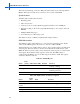
Reset Control register
Primary byte offset: DB:D8h
Secondary byte offset: DB:D8h
3.3V PMC site
The CPU Board supports a two PMC sites on the system board. Each PMC site
uses three PMC connectors. Two connectors (denoted as J11 and J12 on slot A and
J21 and J22 on slot B) carry the 32-bit PCI signals.The third connector (denoted as
J14 on slot A and J24 on slot B) routes the PMC I/O signals. The I/O signals from
slot A are routed to cPCI connector J5 while the I/O signals from slot B are routed
to CompactPCI connector J3.
PMC A has a four 100ohm differential pairs that go to the J5 connector. These
signal are paired as follows:
Pair 1: PMCA 25 and 15
Pair 2: PMCA 29 and 28
Pair 3: PMCA 19 and 18
Pair 4: PMCA 26 and 22
Both PMC sites provide power for 3.3V, 5V, 12V and –12V. The PCI interface uses
3.3V signaling and is keyed for 3.3V operation.
Bit Name R/W Description
0 Secondary Reset R/(WP) Secondary bus reset.
When 0: The 21554 deasserts s_rst_l. This bit
must be cleared by a configuration write in
the case when it is set by a configuration
write. Otherwise, it clears automatically after
100 msec or when p_rst_l deasserts.
When 1: The 21554 asserts s_rst_l. This bit is
set automatically when the Chip Reset bit is
written with a 1 or when p_rst_l is asserted, or
is set with aconfiguration write.
Reset value: 0 (disabled). 1 Chip Reset R/(WP)
1 Chip Reset R/(WP) Chip reset control.
When 1: Causes the 21554 to perform a chip
reset and to assert s_rst_l.
Data buffers, configuration registers, and both
the primary and secondary interfaces are
reset to their initial state. The 21554 clears
this bit once chip reset is complete.
Reset value: 0