EPC -100 Hardware Reference RadiSys Corporation 5445 NE Dawson Creek Drive Hillsboro, OR 97124 Phone: (503) 615-1100 Fax: (503) 615-1150 http://www.radisys.
EPC-100 Hardware Reference Ray-O-Vac is a registered trademark of Ray-O-Vac, Inc. Portions of this manual are Copyright 1993-1994 Cirrus Logic, Inc. IBM, OS/2, and PC/AT are trademarks of International Business Machines Corporation. Intel and Pentium are registered trademarks of Intel Corp. Microsoft and MS-DOS are registered trademarks of Microsoft Corporation. PhoenixBIOS and NuBIOS are trademarks of Phoenix Technologies, Ltd.
EPC-100 Hardware Reference Table of Contents Chapter 1 - Product Description........................................................................1-1 About this Manual ........................................................................................1-1 Overview ......................................................................................................1-3 cPCI bus ......................................................................................................
EPC-100 Hardware Reference IDE Adapter Sub-menu ................................................................................3-5 Type .....................................................................................................3-6 Multi-Sector Transfers .........................................................................3-6 LBA Mode Control ..............................................................................3-6 32-bit I/O.............................................................
EPC-100 Hardware Reference Advanced Chipset Control Sub-menu...........................................................3-17 DRAM Speed.......................................................................................3-17 DMA Aliasing......................................................................................3-17 8-bit I/O Recovery ...............................................................................3-18 16-bit I/O Recovery ............................................................
EPC-100 Hardware Reference Chapter 4 - Theory of Operation .......................................................................4-1 Introduction ..................................................................................................4-1 Block Diagram..............................................................................................4-2 Processor Module Daughterboard.................................................................4-2 Cache Memory ........................................
EPC-100 Hardware Reference Appendix D - Error Messages ............................................................................D-1 Introduction ..................................................................................................D-1 Boot Failures ................................................................................................
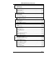
EPC-100 Hardware Reference List of Illustrations Figure 3-1. BIOS Setup Screen Menu Map............................................................... 3-2 Figure 3-2. Main BIOS Setup Menu ......................................................................... 3-3 Figure 3-3. IDE Adapter Sub-Menu. ........................................................................ 3-5 Figure 3-4. Boot Options Sub-menu.......................................................................... 3-8 Figure 3-5.
Product Description Chapter 1 - Product Description About this Manual This manual assumes that the reader has good familiarity with PC sytems based on the Intel x86 architecture and some familiarity with CompactPCI (cPCI) bus architecture. This manual was written to provide detailed hardware reference information for OEMs, system integrators, and others who use the EPC-100 as a component of their cPCI bus systems.
Product Description Appendix A Chipset and I/O Map. Maps the addresses used for I/O and by the chipset registers. Appendix B Interrupts and DMA Channels. Shows the DMA channel and IRQ assignments to the peripherals supported by the EPC-100. Appendix C Connectors. Details the location, form, and pin-outs of the connectors used in the EPC-100. Appendix D Error Messages and Diagnosis. Explanations of common error messages and start-up codes.
Product Description Overview The EPC-100 is a highly integrated PC-compatible computer designed for use in the full 32-bit CompactPCI (cPCI) bus environment. The EPC-100 is a two-slot 6U cPCI bus module that supports up to seven 3U/6U cPCI peripheral slots via a DEC 21150 PCI-PCI bridge chip. It is compatible with all major PC software environments, including Microsoft DOS, Microsoft Windows 95, and NT 4.0, and IBM OS/2, plus others.
Product Description Standard front panel PC peripheral interfaces with standard interface connectors include: • two RS232 serial ports • a bi-directional IEEE 1284 ECP/EPP parallel port • two USB ports • a fast SCSI-II controller with front panel interface • 10/100BaseTX and 10BASE2 Ethernet ports • PS/2 style mouse and keyboard connectors Additional features include: • SVGA interface.
Product Description about PICMG and the cPCI standard consult the PICMG website at http://www.picmg.org. cPCI Device Interface The EPC-100 implements a 32 bit CompactPCI system slot board capable of driving seven CompactPCI slots. A DEC 21150 PCI-PCI bridge chip is used to interface between the base board’s local PCI bus and the CompactPCI bus. The bridge chip controls a layer of buffers between it and the CompactPCI bus and has a glueless interface to the local PCI bus.
Product Description Specifications Environmental Specifications The following are the environmental specifications for the EPC-100.
Product Description Vibration operating 2.5 g acceleration over 5-300 Hz sine wave, 1 oct/min sine sweep without HDD storage 5 g acceleration over 5-2K Hz sine wave, oct/min sine sweep Shock operating 30 g, 11 ms duration, half-sine shock pulse without HDD storage 50 g, 11 ms duration, half-sine shock pulse Vibration operating 0.5mm P-P (5 - 22 Hz) 0.5G (max.) (22 - 400 Hz) with HDD storage 5mm P-P (5 - 22 Hz) 5G (max.
Product Description Other Specifications The following table contains additional specifications. A typical system is assumed, with SVGA and 32 MB of RAM. Characteristic Value Electrical TBD Current +5V 2.6A. typical, depending on processor +12V 0.1A typical +3.3V 3.1A typical, EPC100-100 3.2A typical, EPC 100-133 5.4A typical, EPC-100-166 3.4A typical, EPC-100-200MT -12V 0.2A typical Weight 2.7 lb. (1.3 kg) Dimensions see cPCI Specification Rev. 1.0 for a 6U 2-slot module.
Product Description EMC CE Mark CISPR 11:1990/EN 55011(1991): Group 1 Class A IEC 801-2:1991/EN50082-1 (1992): 4kV CD, 8kV AD IEC 801-3:1984/EN50082-1 (1992): 3V/m IEC 801-4:1988/EN50082-1 (1992): 1kV Power Line Low Voltage Directive 89/336/EEC Table 1-2. Additional EPC-100 Specifications.
Installation Chapter 2 - Installation Introduction This chapter tells you how to install the EPC-100 in a Compact PCI (cPCI) chassis. There are three user-configurable jumpers. One enables/disables the CPU fan failure test during Power On Self-test (POST). The second enables/disables the SCSI termination, so that the EPC-100 can be used as any element in a SCSI daisy-chain. The third jumper determines whether an external floppy disk drive will be powered by the on-board floppy drive connector or not.
Installation Inserting the EPC-100 ! WHEN HANDLING OR INSERTING THE EPC-100 MODULE, AVOID ▲ TOUCHING THE CIRCUIT BOARD AND CONNECTOR PINS, AND MAKE SURE THE ENVIRONMENT IS STATIC-FREE. To install the EPC-100 in the cPCI chassis, make sure that the extractor handles on the front panel are pulled away from each other to their maximum extent. Engage the chassis guides with the EPC-100 and push it in until the extractor handles rest on the latch rail extrusion of the cPCI chassis.
Installation The next step of installation is connecting peripherals, typically a video display and keyboard, and perhaps a mouse, modem, printer, etc. Pin-outs for the EPC-100 front-panel connectors are specified in Appendix C - Connector and Jumpers. SCSI Termination When you configure SCSI peripherals to work with the EPC-100, you need to consider the placement of the EPC-100 in the SCSI chain. If the EPC-100 is to be the last device in the SCSI chain, it must be terminated.
Installation Ethernet Software The Ethernet driver software is supplied on a diskette with part number 80-1677-00 labeled Ethernet Drivers, DEC 21143/Windows NT 4.0. If you need to install a different driver for an operating system other than Windows NT 4.0, consult Digital Equipment Corporation at http://www.digital.com/info/semiconductor/support.htm.
BIOS Configuration Chapter 3 - BIOS Configuration Introduction The EPC-100 uses the Phoenix NuBIOS to configure and select various system options. This section details the various menus and sub-menus that are used to configure the system. This section is written as though you are setting up each field in sequence and for the first time. Your system may be correctly pre-configured and require very little setup.
BIOS Configuration BIOS setup is accomplished by making selections from a series of menus, shown in Figure 3-1. Figure 3-1. BIOS Setup Screen Menu Map. Access to the setup screen is possible only during a short time during bootup when a message is displayed indicating that the "F2" key may be pressed to enter setup. This provides consistency of operation across all supported operating systems, and forces a direct correspondence between the displayed System BIOS setup settings and the hardware.
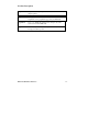
BIOS Configuration Main Setup Menu The Main Setup Menu is shown below: PhoenixBIOS Setup - Copyright 1985-96 Phoenix Technologies Ltd.
BIOS Configuration Video System: This field is used to select the video type. Possible selections are: “EGA/VGA”, “CGA 80x25”, and “Monochrome”. The default is “EGA/VGA”. Memory Cache Sub-menu The term “Memory Cache” refers to the technique of caching BIOS images. See “Memory Cache Sub-menu” on page 3-20 for more information. Memory Shadow Sub-menu The term “Memory Shadow” refers to the technique of copying information from an extension ROM into DRAM and accessing it in this alternate memory location.
BIOS Configuration IDE Adapter Sub-menu There are a total of four IDE adapter sub-menus for the primary and secondary hard disk controllers, each having a master and slave drive screen. The detailed characteristics of the drive connected to the adapter are available in the IDE Adapter 0 sub-menu, which displays the following screen: PhoenixBIOS Setup - Copyright 1985-96 Phoenix Technologies Ltd.
BIOS Configuration Type “None” is selected if there is no IDE hard disk drive for this adapter. In the case for which there is an IDE disk but the “Autotype” feature cannot be employed, then the “User” type is selected and the correct drive values for cylinders, heads, sectors/track, and write precompensation for the drive are entered. Selecting “Auto” for this option causes the System BIOS to automatically autotype the hard disk every time POST is executed. The default is “Auto”.
BIOS Configuration Transfer Mode This option selects the mode that the System BIOS uses to access the hard disk. The selections are: Standard (default) Fast PIO 1 Fast PIO 2 Fast PIO 3 Fast PIO 4 Fast DMA A Fast DMA B Fast DMA F Older hard disks only support “Standard”. Newer hard disks adhering to “Fast ATA” or “Enhanced IDE” specifications may support the fast programmed I/O or DMA modes. Note that autotyping may change this value depending on the transfer modes that the hard disk reports it supports.
BIOS Configuration Boot Options Sub-menu The Boot Options Sub-menu allows changing the boot sequence options. The Boot Options Sub-menu shown in Figure 3-4. Boot Options Sub-menu.displays: PhoenixBIOS Setup - Copyright 1985-96 Phoenix Technologies Ltd.
BIOS Configuration The options are as follows: A: then C: Used to boot from the floppy drive, or if no floppy disk is present in the A: drive, boot from the C: drive. C: then A: Used to boot from the C: drive, or if none is present, boot from the A: drive. C: only: Used to boot from the C: drive without searching for an A: drive. The default is “A: then C:”. The setting chosen here displays in the Boot Sequence Sub-menu prompt.
BIOS Configuration Extended Memory Test: This option enables or disables testing of memory above 1MB during boot-up. To speed up the boot process, disable the extended memory test. The default is “Enabled”.
BIOS Configuration Keyboard Features Menu Use this sub-menu to enable or disable various keyboard features. PhoenixBIOS Setup - Copyright 1985-96 Phoenix Technologies Ltd. Keyboard Features Item Specific Help NumLock: Key Click: Keyboard auto-repeat rate: Keyboard auto-repeat delay: F1 ESC Help Exit [Off] [Disabled] [30/sec] [1/4 sec] ↑↓ Select Item ← → Select Menu , , or selects field. -/+ Change Values Enter Select Sub-Menu F9 Setup Defaults F10 Previous Values Figure 3-5.
BIOS Configuration Keyboard auto-repeat delay: This option is used to set the delay between when a key is pressed and when the autorepeat feature begins. Options are “1/4 sec”, “1/2 sec”, “3/4 sec”, and “1 sec” . The default delay is “1/4 sec”.
BIOS Configuration Advanced Menu The Advanced Menu contains settings for integrated peripherals, memory shadow, cache, and large disk access mode. PhoenixBIOS Setup - Copyright 1985-96 Phoenix Technologies Ltd. Main Advanced Power Exit Warning! Item Specific Help Setting items on this menu to incorrect values may cause your system to malfunction.
BIOS Configuration Plug & Play OS If enabled, this option informs the System BIOS that the operating system that is booted supports Plug and Play. This forces the Plug and Play portion of the System BIOS to only configure motherboard devices and those peripherals that are necessary for booting (display, hard disk, etc.). Thus the operating system must configure the other devices and peripherals. The default is “No”.
BIOS Configuration BIOS Extension Offset in FBD: This option selects the source address of the BIOS extension located in the FBD. The address is an offset from the base of the FBD. The offset range is between 4A000h through 5E000h in 8KB increments. The default is “Disabled”. Destination Address: This option selects the target address of the BIOS extension which can range from CC0000h through DFFFFh in 8KB increments. The default is “D0000h”.
BIOS Configuration Integrated Peripherals Sub-menu The options in this sub-menu are used to configure the onboard serial and parallel port and disk controllers. PhoenixBIOS Setup - Copyright 1985-96 Phoenix Technologies Ltd.
BIOS Configuration LPT port This option is used to configure the parallel port labeled on the front panel as “LPT”. The choices for I/O base addresses and IRQs are: “Disabled”, “378, IRQ7”, “278, IRQ5”, and “Auto”. “Auto” causes the System BIOS to choose a base address and IRQ setting that avoids conflicting with the other ports. The default I/O base and IRQ for this LPT port are “378, IRQ7”. LPT Mode This option sets the mode under which the bi-directional LPT port operates.
BIOS Configuration Advanced Chipset Control Sub-menu The options on this screen allow control over selected chipset settings that affect performance or function. The Advanced Chipset Control Sub-menu is shown below. PhoenixBIOS Setup - Copyright 1985-96 Phoenix Technologies Ltd. Advanced Chipset Control Item Specific Help DRAM Speed: DMA Aliasing: 8-bit I/O Recovery: 16-bit I/O Recovery: IRQ 12 used by: ECC/Parity Config: F1 ESC [70 ns] [Enabled] [4.5] [4.
BIOS Configuration 8-bit I/O Recovery This option selects the number of ISAbus SYSCLKs to be inserted by the chipset between 8-bit back-to-back I/O accesses. Increasing the number of clocks decreases I/O performance but may allow slow devices to be accessed properly. This option can range from 3.5 through 11.5 SYSCLKs in 1 SYSCLK increments. The default is “4.5” SYSCLKs.
BIOS Configuration Memory Cache Sub-menu The options in this screen allow you to control whether or not certain memory regions are cached and whether or not the external Level 2 (L2) cache is enabled or disabled. The Memory Cache Sub-menu is shown below. PhoenixBIOS Setup - Copyright 1985-96 Phoenix Technologies Ltd.
BIOS Configuration Cache Video BIOS Area This option enables or disables caching of the VGA BIOS area in the C0000h through C7FFFh region. The default is “Enabled”. Cache Memory Regions These options enable or disable caching of the associated memory regions. When BIOS extensions are present in these regions, enabling caching for that region increases performance. The default is “Disabled”.
BIOS Configuration Memory Shadow Sub-menu The term “shadowing” refers to the technique of copying BIOS extensions from ROM into DRAM and accessing them from DRAM. This allows the CPU to access the BIOS extensions much more quickly and generally increases system performance if many calls to the BIOS extensions are made. The Memory Shadow Sub-menu is shown below. PhoenixBIOS Setup - Copyright 1985-96 Phoenix Technologies Ltd.
BIOS Configuration Shadow Memory Regions These options enable or disable shadowing for the associated memory region. The default is “Disabled”.
BIOS Configuration Power Management Menu The options in this menu provide control over the power management facilities. As the screen graphic below shows, only about one-half of the Power Management Menu Screen entries are visible at any one time; however, for completeness, all of the Power Management Menu entries are listed and annotated below. System BIOS Power Management supported states are: Fully On, Standby Mode (partial power reduction), and Suspend Mode (maximum power reduction).
BIOS Configuration Standby Timeout This option enables and sets the inactivity duration required to elapse before the system is placed into Standby Mode, or it disables the Standby Timeout. The options are: “Off”, “2 min”, “15 min”, “30 min”, “1 hour”, “2 hours”, “3 hours”, and “4 hours”. The default is “Off”. Auto Suspend Timeout This option enables and sets the inactivity duration required to elapse before the system is placed into Suspend Mode from Standby Mode, or it disables the Suspend Timeout.
BIOS Configuration IRQ5 (System Event, unused) This option enables or disables the System Event for IRQ5. The options are: “Disabled” and “Enabled”. The default is “Disabled”. IRQ6 (System Event, Floppy Disk Drive) This option enables or disables the System Event for IRQ6. The options are: “Disabled” and “Enabled”. The default is “Disabled”. IRQ7 (System Event, LPT1) This option enables or disables the System Event for IRQ7. The options are: “Disabled” and “Enabled”. The default is “Disabled”.
BIOS Configuration IRQ14 (System Event, Primary IDE Controller) This option enables or disables the System Event for IRQ14. The options are: “Disabled” and “Enabled”. The default is “Disabled”. IRQ15 (System Event, unused or MIRQ for Secondary IDE Controller) This option enables or disables the System Event for IRQ15. The options are: “Disabled” and “Enabled”. The default is “Disabled”. SMI (System Event, Power Management or Watchdog Timer Event) This option enables or disables the System Event for SMI.
BIOS Configuration Exit Menu The options in this menu allow saving settings and exiting, or abandoning changes and exiting to the system, or controlling the backup and restoration of CMOS RAM to the FBD. PhoenixBIOS Setup - Copyright 1985-96 Phoenix Technologies Ltd.
BIOS Configuration Backup CMOS to Flash This option is used to immediately save current Setup settings to CMOS RAM and into FBD main block #1. Restore CMOS from Flash This option is used to immediately restore CMOS RAM and update current Setup settings from FBD main block #1. Restore CMOS Condition This option is used to determine under what conditions the System BIOS restores CMOS RAM from FBD main block #1 when booting. The restore conditions are: “Always”, “Never”, and “CMOS Corruption”.
Theory of Operation Chapter 4 - Theory of Operation Introduction The EPC-100 is a double-slot 6U size module designed to the cPCI Revision 1.0 specification.
Theory of Operation EIDE Controller consisting of two master and two slave drive controllers System BIOS implemented as a Flash ROM supporting BIOS extensions Block Diagram Figure 4-1 shows the division and interconnection of EPC-100 functions. These are described below. Processor Module Daughterboard An Intel Pentium processor (with integral FPU) runs at 100, 133, 166, or 200 MHz. The processor, the TXC system controller, and the L2 cache all operate on a 60/66MHz local bus.
Theory of Operation Figure 4-1. Block Diagram of the EPC-100.
Theory of Operation Upgrading Main System Memory At the time of writing, the the following sizes of 60 or 70ns Fast Page Mode or EDO DRAM were useable: Type Row/Column Total Size (MB) Number of SODIMMs 512Kx32 10/9 4 2 1Mx32 10/9 or 10/10 8 2 2Mx32 10/10 or 10/11 16 2 4Mx32 11/10, 11/11, or12/10 32 2 4Mx32 11/10, 11/11, or12/10 64 4 8Mx32 12/11 128 4 16Mx32 12/12 256 4 Table 4-1. Memory Upgrade DRAMs.
Theory of Operation Range 00000000 - 0009FFFF 000A0000 - 000BFFFF 000C0000 - 000C7FFF 000C8000 - 000CFFFF 000D0000 - 000DFFFF 000E0000 - 000FFFFF 10000000 - FFF7FFFF FFF80000 - FFFFFFFF Content First 640 KB of DRAM (DOS memory) VGA video DRAM, mapped to the Video Module Write-protected DRAM containing shadowed video BIOS SCSI BIOS extension BIOS Extensions System BIOS Shadow ISA Bus (aliased) BIOS Cacheable yes no yes yes yes yes no no Table 4-2. System Memory Map.
Theory of Operation Interrupt Interrupt Function IRQ10 unused IRQ11 unused IRQ12 Mouse IRQ13 Numeric coprocessor FERR# (internal PIIX3 connection) IRQ14 Primary IDE IRQ15 unused (MIRQ0 for secondary IDE) NMI PIIX3 when SERR# or IOCHK# is asserted (software controlled) SMI Power management / Watchdog Timer Event.
Theory of Operation watchdog time-out caused the hardware reset (as opposed to SYSRESET or poweron reset). Depending on the value of a setup option the BIOS will then either HALT the CPU or allow the boot process to continue. Service of a watchdog interrupt is signaled to the counter by writing the register at I/O 8150h. This will reset the counter and reset the signal driving IRQ9. Flash Boot Device The Intel E28F004BX-T is used as a Flash Boot Device (FBD).
Theory of Operation BIOS ROM and ROM Shadowing The EPC-100 utilizes a Flash Boot Device (FBD) as its BIOS ROM. The BIOS ROM is mapped into the top of the processor’s 32-bit address space. The BIOS consists of a 16 KByte boot block and the System BIOS in the 96KB Main block and both 8KB parameter blocks. The layout is described in Figure 4-2.
Theory of Operation The BIOS initialization software copies the ROM contents into DRAM (a process called shadowing) at addresses E0000h-FFFFFh. The VGA BIOS is copied into C0000h-C7FFFh of DRAM. After copying into these areas, the BIOS write-protects them. Subsequent writes to these areas complete successfully but do not alter the data in DRAM. There are two parameter blocks, each 8KB in size, used for BIOS code.
Theory of Operation Battery The battery powers the CMOS RAM and TOD clock when system power is not present. At 60°C, the battery should have a shelf life of over four years. In a system that is powered on much of the time and where the ambient power-off temperature is less than 60°C, the battery is estimated to have a life of 10 years. If system power is present, the +5V voltage also powers the CMOS RAM and TOD clock.
Theory of Operation Figure 4-3. Replacing the Lithium CMOS Battery. + CAUTION: There is danger of explosion if battery is incorrectly replaced. Replace only with same or equivalent type recommended by RadiSys. Dispose of used batteries according to manufacturer’s instructions. Peripheral Ports The I/O address and IRQ of the peripheral ports are determined by the CMOS parameters established by default and modified via BIOS Setup screens.
Theory of Operation Address Block Name Notes 03F0-03F1h Configuration Write only1,2 03F0-03F1h Floppy Disk Read only2 03F2-03F5h, 03F7h Floppy Disk 2 03F8-03FFh Serial Port, COM1 2 02F8-02FFh Serial Port, COM2 2 0278-027Ah Parallel Port, LPT1 2 01F0-01F7h, 03F6h, 03F7h IDE (not used) AT Mode2,3 Table 4-4. Super I/O Chip Address Blocks. Notes: 1 Configuration registers can only be modified by writing a security code sequence to 3F0h.
Theory of Operation Parallel Port The printer port is a bi-directional IEEE1284-C PC parallel port. The parallel port supports bi-directional communication compatible with the PS/2 definition. It is configured as LPT1 and mapped to I/O address 378h-37Fh and uses interrupt IRQ7. If not needed, LPT1 can be disabled in the BIOS Setup Integrated Peripherals SubMenu to free up the I/O address and interrupt for usage by other expansion products.
Theory of Operation registers are located as function 2 of the PIIX3 configuration space and utilize PCI INTD. Front Panel Indicators 6 LEDs on the front panel are used as system activity indicators: RUN (green) The RUN LED is lit whenever a write access to DRAM is made. This provides a normally lit LED indicating that the CPU is running. It is not lit if the CPU is halted or is executing entirely out of the on-chip cache.
Support and Service Chapter 5 Support and Service In North America Technical Support RadiSys maintains a technical support phone that is staffed weekdays (except holidays) between 8:00 AM and 5:00 PM Pacific time. If you require assistance outside these hours, you can leave a message on voice-mail using the same phone number. You can also request help via electronic mail or by FAX addressed to RadiSys Technical Support Department. See the cover of this manual for the RadiSys telephone and FAX numbers.
Support and Service Repair Services RadiSys provides Factory Repair Service for the entire RadiSys product line. Standard service for all RadiSys products covers factory repair with customers paying shipping to the factory and RadiSys paying for return shipment. Overnight return shipment is available at customer expense. Normal turn-around time for repair and re-certification is five working days.
Support and Service RadiSys provides a recertification service for products either in or out of warranty. This service verifies correct operation of a product by inspecting and testing the product using standard manufacturing tests. There is a product-dependent charge for recertification. Generally, very few components are field-repairable. However, since RadiSys understands that some customers want or need the option of repairing their own equipment, all components are available in a spares program.
Support and Service Other Countries Use the RadiSys web site to contact us, or contact the sales organization from which you purchased your RadiSys product for service and support.
Chipset and I/O Map Appendix A - Chipset and I/O Map Introduction This section contains the port I/O addresses for the address-mapped devices in the EPC-100. As is standard for the ISA bus, the A[15:0] bits are decoded for the 0200h-03FFh range and A[15] and A[9:0] are decoded for addresses above 8000h. Table A-1.
Chipset and I/O Map First (8-bit) DMA controller (cont’d) I/O Addr Functional group 00D Usage Temporary register (R) Master clear (W) 00E Clear mode reg counter (R) Clear all DMA req mask(W) 00F 020 021 040 All DMA request mask First Interrupt controller Interrupt controller 1 Port 0 Port 1 Counter-Timer functions Timer Counter 0 041 Counter 1 042 Counter 2 043 Control (W) Keyboard Port 060 Keyboard controller 061 NMI status 064 Keyboard controller EPC-100 Hardware Reference Data I/O
Chipset and I/O Map Time-of-Day Clock I/O Addr Functional group Usage 070 Real-time clock RTC index reg / NMI enable 071 RTC data register (64 bits) 0 seconds 1 seconds alarm 2 minutes 3 minutes alarm 4 hours 5 hours alarm 6 day of week 7 date of month 8 month 9 year A status A B status B C status C D status D E…3F RAM Phoenix NuBIOS 080 EPC-100 Hardware Reference Phoenix BIOS Status Information A-3
Chipset and I/O Map DMA Page Registers I/O Addr Functional group 081 DMA Usage Channel 2 page register 082 Channel 3 page register 083 Channel 1 page register 087 Channel 0 page register 089 Channel 6 page register 08A Channel 7 page register 08B Channel 5 page register 08F Refresh page register Second Interrupt Controller 0A0 Interrupt controller 2 0A1 Port 0 Port 1 Power Management Controller 0B2 Power Management 0B3 Control Status DMA Controller 0C0 DMA Channel 4 address 0C
Chipset and I/O Map DMA Controller (cont’d) I/O Addr Functional group 0D4 Usage Command register (R) Single-bit DMA req mask(W) 0D6 Mode 0D8 Set byte pointer (R) Clear byte pointer (W) 0DA Temporary register (R) Master clear (W) 0DC Clear mode reg counter (R) Clear all DMA req mask (W) 0DE All DMA request mask 0E0 Phoenix BIOS Status Information Coprocessor Interface 0F0 Coprocessor Clear coprocessor busy 0F1 Reset coprocessor IDE Control 170 172 173 174 175 176 177 1F0 1F2 1F3 1F4 1F5
Chipset and I/O Map ISA Plug and Play I/O Addr Functional group 279 Plug and Play Usage A79 Data Register CF8 Configuration Address Register CF9 Turbo reset control register CFC Configuration data register Serial I/O (COM B) Port 2F8 COM B serial port Receiver/transmitter buffer Baud rate divisor latch (LSB) 2F9 Interrupt enable register Baud rate divisor latch (MSB) 2FA Interrupt ID register 2FB Line control register 2FC Modem control register 2FD Line status register 2FE Modem
Chipset and I/O Map VGA I/O Addr Functional group 3B4 VGA Usage CRT Controller index 3B5 CRT Controller data 3BA Feature control output, Input status 3C0 Attribute controller Index/Data 3C1 Attribute controller Index/Data 3C2 Miscellaneous output, Input status 3C3 Sleep 3C4 Sequencer Index 3C5 Sequencer Data 3C6 Video DAC pixel mask, Hidden DAC register 3C7 Pixel address read mode, DAC state 3C8 Pixel mask write mode 3C9 Pixel data 3CA Feature control readback 3CC Miscellane
Chipset and I/O Map Serial I/O (COM A) Port I/O Addr Functional group 3F8 COM A serial port Usage Receiver/transmitter buffer Baud rate divisor latch (LSB) 3F9 Interrupt enable register 3FA Interrupt ID register 3FB Line control register 3FC Modem control register 3FD Line status register 3FE Modem status register Baud rate divisor latch (MSB) Interrupt Control Registers 4D0 Interrupt 4D1 PIIX3 Edge/ level control - Int1 PIIX3 Edge/ level control - Int2 ECP Registers 778 ECP Data FI
Chipset and I/O Map ENIE ENUM# interrupt enable. If 1, the cPCI signal ENUM# is allowed to generate a hotswap event which will generate an interrupt (if the watchdog interrupt is also disabled). If 0, no hotswap events are signaled. Power up and reset state: 0. ENEV Read only bit that indicates a hotswap (ENUM#) event occurred. A high indicates a hotswap event occurred. Any write to I/O locations 8150-815Fh will reset this bit. Power up and reset state: 0.
Chipset and I/O Map If you are using the watchdog timer, it is required to write to this register within the defined period of the timer to prevent generating either an interrupt or a warm reset.
Interrupts Appendix B - Interrupts Interrupt Source IRQ0 Timer IRQ1 Keyboard Controller IRQ2 Cascade Interrupt Input IRQ3 COM B, COM A, or Unassigned IRQ4 COM A, COM B, or Unassigned IRQ5 Unassigned IRQ6 Floppy Disk or Unassigned IRQ7 LPT1: or Unassigned IRQ8 Real Time Clock IRQ9 Watchdog Timer IRQ10 Unassigned IRQ11 Unassigned IRQ12 PS/2 Mouse IRQ13 Floating Point Unit IRQ14 Primary IDE IRQ15 Secondary IDE NMI ISAbus IOCCHK/Memory Parity Error SMI Power Management/ECC/
Connectors Appendix C - Connectors and Jumpers Introduction This section details the connectors and jumpers used by the EPC-100 and gives the signal pinout of each connector. 581 ,'( 1(7 5(6(7 &3&, 6&6, 1(7 9*$ 6&6, &20 $ %$6( &20 % %$6(7; %$6(7; 86% .%' /37 0286( Figure C-1. EPC-100 Front Panel Connectors.
Connectors Keyboard Connector The PS/2 keyboard connector is a 6-pin mini-DIN connector defined as follows: Pin 1 2 3 Signal Data not used Ground Pin 4 5 6 Signal +5V Clock not used Table C-1. Keyboard Pin-Out. Mouse Connector The PS/2 mouse connector is a 6-pin mini-DIN connector defined as follows: Pin 1 2 3 Signal Data not used Ground Pin 4 5 6 Signal +5V Clock not used Table C-2. Mouse Pin-Out.
Connectors RS-232 Ports (COM A, COM B) The RS-232 serial port male DB-9 DTE connectors are defined as follows: Pin 1 2 3 4 5 Signal Carrier detect Receive data Transmit data Data terminal ready Signal Ground Pin 6 7 8 9 Signal Data set ready Request to send Clear to send Ring indicator Table C-3. DB-9 Pin-Out.
Connectors SVGA Connector The SVGA monitor port is a DB-15 connector defined as follows: Pin 1 2 3 4 5 6 7 8 Signal Red Green Blue (not used) Ground Ground Ground Ground Pin 9 10 11 12 13 14 15 Signal (key) Ground (not used) (not used) Horizontal sync Vertical sync programmable output Table C-5. DB-15 Pin-Out.
Connectors Dual USB Connector The USB (Universal Serial Bus) connector is a dual, stacked 4-pin connector defined as follows: Pin Mechanical Solder Lug 1 2 3 4 Mechanical Solder Lug Description Shield Ground VCC (1Amp Fused) DATADATA+ Signal Ground Shield Ground Table C-7.
Connectors SCSI-2 Connector The SCSI-2 port is a female 50-conductor .050 center mini-D style connector defined in the following table. To disable the SCSI terminator, see SCSI Terminator Disable Jumper, later in this appendix.
Connectors EIDE (Primary) Connector The Primary EIDE Connector is a male 44-pin right-angle header. If an optional hard disk drive is installed, it is installed on the primary channel. A slave drive may be attached also using a ribbon cable (user supplied). The optional hard disk is 2.5” style using power supplied by pins 41-44 of the connector. If you wish to connect a 40-pin connector, omit these power supply lines.
Connectors Floppy Disk Drive Connector The Floppy disk drive connector is a male 34-pin. The pins and signals are defined in the following table: Pin 1 3 5 7 9 11 13 15 17 19 21 23 25 27 29 31 33 Signal GND N.C. N.C. Vcc* Vcc* Vcc* GND GND GND GND GND GND GND GND GND GND GND Pin 2 4 6 8 10 12 14 16 18 20 22 24 26 28 30 32 34 Signal DENSEL N.C. RATE0 INDEX MTR1 DS0 DS1 MTR0 DIR STEP WDATA WGATE TRK0 WRPRT RDATA HDSEL DSKCHG * - Vcc if jumper JP2 is installed (RadiSys floppy drive) N.C.
Connectors CompactPCI J1 & J2 Connectors The CompactPCI J1connector is a female 2mm-pitch 6 column by 25 row right angle Hard Metric (HM) connector. The CompactPCI J2 connector is exactly the same as the J1 connector except there are only 22 rows numbered 26-47. All of these signals have the standard CompactPCI revision 1.0 bus definitions. The symbol * before or after a signal indicates a note exists for this signal on the next page.
Connectors CompactPCI J1 Connector* Pin A B C D * E F C/BE[0]# GND 21 3.3V AD[9] AD[8] M66EN 22 AD[7] GND 3.3V AD[6] AD[5] GND 23 3.3V AD[4] AD[3] 5V AD[2] GND 24 AD[1] 5V V(I/O) AD[0] ACK64# GND 25 5V REQ64# BRSV 3.
Connectors CompactPCI J2 Connector* Pin A B C D E F 44 USR USR USR USR USR GND 45 USR USR USR USR USR GND 46 USR USR USR USR USR GND 47 USR USR USR USR USR GND × Notes: 1. This diagram defines the pinout from the front of the system chassis. All pins are medium length (level 2) except C16 and D15 which are long (level 3) and short (level 1), respectively. The V(I/O) signals are either 5V or 3.3V, depending on the system implementation. 2.
Connectors Fan Failure Detect Enable Jumper The Fan Failure Detect Enable Jumper, labelled Fail Fail Conn, is located at the bottom of the Main board, behind the front panel mouse connector as shown in Figure C-1. The jumper is installed to enable detection of fan failure during POST. SCSI Terminator Disable Jumper The SCSI Terminator Disable Jumper is located behind the top ejector on the Main board. To disable the SCSI terminator, apply a jumper.
Error Messages Appendix D - Error Messages Introduction Boot Failures The System BIOS attempts to display an error message on the VGA and halts when it encounters the following error conditions: 1. 2. Fixed disk error • No drive connected • Configured for 0 cylinders • Controller reset failed • Drive not ready • Track 0 seek timed out • Drive initialization failed • Drive recalibration failed • Last track seek failed Video error • 3. Timer error • 4.
Error Messages 5. I/O chip error • 6. I/O conflicts exist for serial and parallel ports, floppy, hard disk (any or all) Other error • IRQ conflict, unsupported COM port configuration, keyboard locked • Pentium cooling fan has failed The System BIOS prints an error message but does not halt when it encounters the following error conditions: 1. 2.