
User's Manual

Honeywell Confidential and Proprietary Revision –1.1 Page 7 of 15
Copyright © 2015 Honeywell Analytics, All rights reserved.
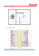
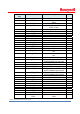
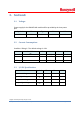
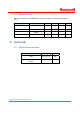
Connector
Pin
Pin Name Description I/O
1,2,4,24 GND Ground
3 RESET Active-low system reset for
Micro
I
5 UART1_TXD UART1 transmit output O
7 HM0/Bootstrap Enable/Disable into boot load /
UART receive
I
9 GPIO16 General purpose IO I/O
11 UART1_RXD UART1 receive input I
13 USB_DN USB Data Minus I/O
15 USB_DP USB Data Plus I/O
17 GPIO17 General purpose IO I/O
19 WakeUp I/O
21 DAC0 DAC Input I/O
23 I2S0_WS I2S0 Word select I/0
25 I2S0_SDO I2S0 serial data output O
27 PTB17 GPIO I/O
29 PTB16 GPIO I/O
31 SPI_MISO Slave SPI master in slave out
line
I/O
33 SPI_MOSI Slave SPI master out slave in
line
I/O
35 SPI_CLK Slave SPI clock line I
37 SPI_CS/HM1 Slave SPI chip select line/
Enable/Disable into boot load
I
22,39,40 VCC Power Supply to module
6 UART0_TXD UART0 transmit output O
8 UART0_RXD UART0 receive input I
10 UART0_RTS RTS input (Request To Send) for
UART hardware flow control
I/O
12 UART0_CTS CTS output (Clear To Send) for
UART hardware flow control
I/O
14 I2S0_SDI I2S0 Serial data input I
16 I2C_SDA I2C Serial data I/O
18 I2C_SCL I2C Serial clock I/O
20 GPIO18 GPIO I/O
26 ADC_DP ADC Data line to micro I/O
28 ADC_DM ADC Data line to micro I/O
30 POWERDOWN_OUT
32 I2C_CLK I2C Clock I/O
34 UART1_RXD UART1 receive input I
36 TD0
38 UART0_RXD / I2C
Data
UART0 receive input / I2C Serial
Data
I, I/O