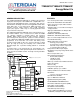
9-5376; Rev 1.1; 4/11 71M6541D/71M6541F/71M6542F Energy Meter ICs A Maxim Integrated Products Brand DATA SHEET April 2011 GENERAL DESCRIPTION FEATURES The 71M6541D/71M6541F/71M6542F are Teridian’s 4th-generation single-phase metering SoCs with a 5MHz 8051-compatible MPU core, low-power RTC with digital temperature compensation, flash memory, and LCD driver.
Table of Contents 1 2 3 2 Introduction ................................................................................................................................. 10 Hardware Description .................................................................................................................. 11 2.1 Hardware Overview............................................................................................................... 11 2.2 Analog Front End (AFE) ...................................
.3 4 5 6 v1.1 Fault and Reset Behavior ...................................................................................................... 85 3.3.1 Events at Power-Down .............................................................................................. 85 3.3.2 IC Behavior at Low Battery Voltage ........................................................................... 86 3.3.3 Reset Sequence ................................................................................................
6.1 6.2 6.3 6.4 Absolute Maximum Ratings ................................................................................................. 138 Recommended External Components ................................................................................. 139 Recommended Operating Conditions .................................................................................. 139 Performance Specifications .................................................................................................
Figures Figure 1: IC Functional Block Diagram ..................................................................................................... 9 Figure 2. 71M6541D/F AFE Block Diagram (Local Sensors) .................................................................. 12 Figure 3. 71M6541D/F AFE Block Diagram with 71M6x01 ..................................................................... 13 Figure 4. 71M6542F AFE Block Diagram (Local Sensors) ...........................................................
Tables Table 1. Required CE Code and Settings for Local Sensors................................................................... 15 Table 2. Required CE Code and Settings for 71M6x01 isolated Sensor ................................................. 15 Table 3: ADC Input Configuration ......................................................................................................... 17 Table 4: Multiplexer and ADC Configuration Bits ....................................................................
Table 54: Data/Direction Registers for SEGDIO16 to SEGDIO31 (71M6542F) ....................................... 64 Table 55: Data/Direction Registers for SEGDIO32 to SEGDIO45 (71M6542F) ....................................... 64 Table 56: Data/Direction Registers for SEGDIO51 to SEGDIO55 (71M6542F) ....................................... 64 Table 57: LCD_VMODE[1:0] Configurations .......................................................................................... 65 Table 58: LCD Configurations .......
Table 107: PLL Performance Specifications ......................................................................................... 144 Table 108: LCD Driver Performance Specifications .............................................................................. 145 Table 109: LCD Driver Performance Specifications .............................................................................. 146 Table 110: VREF Performance Specifications......................................................................
VREF IAP IAN IBP IBN V3P3A GNDA GNDD VLCD V3P3SYS ∆Σ AD CONVERTER VBIAS MUX and PREAMP VBIAS VLCD Voltage Boost FIR V3P3A - V3P3D + VREF VA VB* VREF VBAT MUX MUX CTRL CROSS Voltage Regulator CK32 XIN XOUT MCK PLL RTCLK (32KHz) Oscillator CK32 32KHz 32 KHz DIV ADC 4.9 MHZ CKADC VDD 4.9 MHz CKFIR 22 2.5V to logic CLOCK GEN CK_4X MUX LCD_GEN CKMPU_2x WPULSE STRT VARPULSE CKCE < 4.9MHz LCD DRIVER RTM 32-bit Compute Engine TEST MODE CEDATA 32 0x000...
1 Introduction This data sheet covers the 71M6541D (32KB), 71M6541F (64KB) and 71M6542F (64KB) fourth generation Teridian energy measurement SoCs. The term “71M654x” is used when discussing a device feature or behavior that is applicable to all three part numbers. The appropriate part number is indicated when a device feature or behavior is being discussed that applies only to a specific part number. This data sheet also covers basic details about the companion 71M6x01 isolated current sensor device.
2 Hardware Description 2.1 Hardware Overview The Teridian 71M6541D/F and 71M6542F single-chip energy meter ICs integrate all primary functional blocks required to implement a solid-state residential electricity meter.
transformers (CTs) and their corresponding signal conditioning circuits can be characterized and their correction factors can be programmed to produce electricity meters with exceptional accuracy over the industrial temperature range. One of the two internal UARTs is adapted to support an Infrared LED with internal drive and sense configuration and can also function as a standard UART. The optical output can be modulated at 38 kHz.
Figure 3 shows the 71M6541D/F multiplexer interface with one local and one remote resistive shunt sensor. As seen in Figure 3, when a remote isolated shunt sensor is connected via the 71M6x01, the samples associated with this current channel are not routed to the multiplexer, and are instead transferred digitally to the 71M6541D/F via the digital isolation interface and are directly stored in CE RAM. See Figure 6 for the multiplexer timing sequence corresponding to Figure 3.
Figure 5 shows the 71M6542F multiplexer interface with one local and one remote resistive shunt sensor. As seen in Figure 5, when a remote isolated shunt sensor is connected via the 71M6x01, the samples associated with this current channel are not routed to the multiplexer, and are instead transferred digitally to the 71M6542F via the digital isolation interface and are directly stored in CE RAM. See Figure 6 for the multiplexer timing sequence corresponding to Figure 5.
is useful when current sensors with low sensitivity, such as shunt resistors, are used. With PRE_E set, the IAP-IAN input signal amplitude is restricted to 31.25 mV peak. For the 71M654x application utilizing two shunt resistor sensors (Figure 3), the IAP-IAN pins are configured for differential mode to interface to a local shunt by setting the DIFFA_E control bit.
I/O RAM Mnemonic FIR_LEN[1:0] ADC_DIV PLL_FAST MUX_DIV[3:0] MUX0_SEL[3:0] MUX1_SEL[3:0] MUX2_SEL[3:0]1 MUX3_SEL[3:0]1 RMT_E DIFFA_E DIFFB_E EQU[2:0] I/O RAM Location 210C[2:1] 2200[5] 2200[4] 2100[7:4] 2105[3:0] 2105[7:4] 2104[3:0] 2104[7:4] 2709[3] 210C[4] 210C[5] 2106[7:5] CE Code -- Equations -- Current Sensor Type -- Applicable Figure -- 71M6541D/E 71M6542F (hex) (hex) 1 1 1 1 1 1 3 3 0 0 A A 1 9 1 1 1 1 1 1 0 0 0 or 1 0, 1 or 2 CE41B0162012 CE41B0166013 0, 1 0, 1 and 2 1 Local Shunt 1 Local S
For both multiplexer sequences shown in Figure 6 and Figure 7, the frame duration is 13 CK32 cycles (where CK32 = 32768 Hz), therefore, the resulting sample rate is 32768 Hz / 13 = 2520.6 Hz. Table 3 summarizes the various AFE input configurations. Multiplexer Frame Settle MUX_DIV[3:0] = 3 Conversions CK32 MUX STATE S Fig. 2: Fig. 3: Fig.
MUX_CTRL launches each pass of the CE through its code. Conceptually, MUX_CTRL is clocked by CK32, the 32768 Hz clock from the PLL block. The behavior of the MUX_CTRL circuit is governed by: • • • • CHOP_E[1:0] (I/O RAM 0x2106[3:2]) MUX_DIV[3:0] (I/O RAM 0x2100[7:4]) FIR_LEN[1:0] (I/O RAM 0x210C[2:1]) ADC_DIV (I/O RAM 0x2200[5]) The duration of each multiplexer state depends on the number of ADC samples processed by the FIR as determined by the FIR_LEN[1:0] (I/O RAM 0x210C[2:1] control field.
Table 4 summarizes the I/O RAM registers used for configuring the multiplexer, signals pins, and ADC. All listed registers are 0 after reset and wake from battery modes, and are readable and writable.
360o - θ, resulting in the residual phase error between the current and its corresponding voltage of θ – Ф. The residual phase error is negligible, and is typically less than ±1.5 milli-degrees at 100Hz, thus it does not contribute to errors in the energy measurements. When using remote sensors, the CE performs the same delay compensation described above to align each voltage sample with its corresponding current sample.
A Vinp B A Vinn B A + G - Voutp B A Voutn B CROSS Figure 8: General Topology of a Chopped Amplifier It is assumed that an offset voltage Voff appears at the positive amplifier input.
2.2.8 71M6x01 Isolated Sensor Interface (Remote Sensor Interface) 2.2.8.1 General Description Non-isolating sensors, such as shunt resistors, can be connected to the inputs of the 71M654x via a combination of a pulse transformer and a 71M6x01 IC (a top-level block diagram of this sensor interface is shown in Figure 36). The 71M6x01 receives power directly from the 71M654x via a pulse transformer and does not require a dedicated power supply circuit.
111 Reserved Notes: 1. Only two codes of RCMD[4:2] (SFR 0xFC[4:2]) are relevant for normal operation. These are RCMD[4:2] = 001 and 010. Codes 000 and 101 are invalid and will be ignored if used. The remaining codes are reserved and must not be used. 2. For the RCMD[1:0] control field, codes 01, 10 and 11 are valid and 00 is invalid and must not be used.
Name WAKE RST Default Default 000 000 Address TMUXRB[2:0] 270A[2:0] RMT_RD[15:8] 2602[7:0] RMT_RD[7:0] 2603[7:0] 0 R/W Description R/W The TMUX bits for control of the isolated sensor. 0 R The read buffer for 71M6x01 read operations. Controls how the 71M654x drives the 71M6x01 power pulse. When set, the power pulse is driven 210C[3] RFLY_DIS 0 0 R/W high and low. When cleared, it is driven high followed by an open circuit flyback interval.
SUM_SAMPS[12:0] supports an accumulation scheme where the incremental energy values from up to SUM_SAMPS[12:0] multiplexer frames are added up over one accumulation interval. The integration time for each energy output is, for example, SUM_SAMPS[12:0]/2520.6 (with MUX_DIV[3:0] = 011, I/O RAM 0x2100[7:4] and FIR_LEN[1:0] = 10, I/O RAM 0x210C[2:1]). CE hardware issues the XFER_BUSY interrupt when the accumulation is complete. 2.3.
CK32 MUX_SYNC MUX_STATE S CKTEST 0 31 FLAG 1 30 31 0 FLAG 1 30 31 SIG N 30 L SB 1 SIG N 0 FLAG L SB RTM DATA0 (32 bits) RTM DATA1 (32 bits) RTM DATA2 (32 bits) RTM DATA3 (32 bits) 31 SIG N 30 L SB 1 L SB 0 FLAG SIG N RTM Figure 10: RTM Timing ADC MUX Frame ADC TIMING MUX_DIV Conversions, MUX_DIV=4 is shown Settle CK32 150 MUX_SYNC MUX STATE 0 S 1 2 S 3 ADC EXECUTION ADC0 CE TIMING 0 ADC1 450 900 ADC2 ADC3 1350 1800 CE_EXECUTION CK COUNT = CE_CYCLES + 1CK for e
2.3.6 Pulse Generators The 71M6541D/F and 71M6542F provide four pulse generators, VPULSE, WPULSE, XPULSE and YPULSE, as well as hardware support for the VPULSE and WPULSE pulse generators. The pulse generators can be used to output CE status indicators, SAG for example, to DIO pins. All pulses can be configured to generate interrupts to the MPU. The polarity of the pulses may be inverted with control bit PLS_INV (I/O RAM 0x210C[0]).
If the FIFO is enabled (i.e., PLS_INTERVAL[7:0] ≠ 0), hardware also provides a maximum pulse width feature in control register PLS_MAXWIDTH[7:0] (I/O RAM 0x210A) . By default, WPULSE and VPULSE are negative pulses (i.e., low level pulses, designed to sink current through an LED).
channel is a 71M6x01 isolated sensor, the sample data does not pass through the 71M6541D/F multiplexer, as seen in Figure 3. In this case, the sample is taken during the second half of the multiplexer cycle and the data is directly stored in the corresponding CE RAM location as indicated in Figure 3. The timing relationship between the remote current sensor channel and its corresponding voltage is precisely defined so that delay compensation can be properly applied by the CE.
IB VA IA 122.07 µs 30.5 µs 122.07 µs 122.07 µs Multiplexer Frame (13 x 30.518 µs = 396.7 µs -> 2520.6 Hz) MUX_DIV[3:0] = 3 Conversions Settle CK32 (32768 Hz) MUX STATE S 0 1 S 2 Figure 14: Samples from Multiplexer Cycle (MUX_DIV[3:0] = 3) VB IB VA IA 91.5 µs 91.5 µs 91.5 µs 30.5 µs 91.5 µs Multiplexer Frame (13 x 30.
2.4 80515 MPU Core The 71M6541D/F and 71M6542F include an 80515 MPU (8-bit, 8051-compatible) that processes most instructions in one clock cycle. Using a 4.9 MHz clock results in a processing throughput of 4.9 MIPS. The 80515 architecture eliminates redundant bus states and implements parallel execution of fetch and execution phases. Normally, a machine cycle is aligned with a memory fetch, therefore, most of the 1-byte instructions are performed in a single machine cycle (MPU clock cycle).
The 80515 writes into external data memory when the MPU executes a MOVX @Ri,A or MOVX @DPTR,A instruction. The MPU reads external data memory by executing a MOVX A,@Ri or MOVX A,@DPTR instruction (PDATA, SFR 0xBF, provides the upper 8 bytes for the MOVX A,@Ri instruction). Internal and External Memory Map Table 10 shows the address, type, use and size of the various memory components.
An alternative data pointer is available in the form of the PDATA register (SFR 0xBF), sometimes referred to as USR2). It defines the high byte of a 16-bit address when reading or writing XDATA with the instruction MOVX A,@Ri or MOVX @Ri,A. Internal Data Memory Map and Access The Internal data memory provides 256 bytes (0x00 to 0xFF) of data memory. The internal data memory address is always 1 byte wide. Table 11 shows the internal data memory map.
2.4.3 Generic 80515 Special Function Registers Table 13 shows the location, description and reset or power-up value of the generic 80515 SFRs. Additional descriptions of the registers can be found at the page numbers listed in the table.
Accumulator (ACC, A, SFR 0x E0): ACC is the accumulator register. Most instructions use the accumulator to hold the operand. The mnemonics for accumulator-specific instructions refer to accumulator as A, not ACC. B Register (SFR 0xF0): The B register is used during multiply and divide instructions. It can also be used as a scratch-pad register to hold temporary data.
Table 15: Port Registers (SEGDIO0-15) SFR Name P0 P1 P2 P3 SFR Address D7 0x80 0x90 0xA0 0xB0 D6 D5 D4 D3 DIO_DIR[3:0] DIO_DIR[7:4] DIO_DIR[11:8] DIO_DIR[15:12] D2 D1 D0 DIO[3:0] DIO[7:4] DIO[11:8] DIO[15:11] Ports P0-P3 on the chip are bi-directional and control SEGDIO0-15. Each port consists of a Latch (SFR P0 to P3), an output driver and an input buffer, therefore the MPU can output or read data through any of these ports.
• • UART0 RX: Serial input data are applied at this pin. Conforming to RS-232 standard, the bytes are input LSB first. UART0 TX: This pin is used to output the serial data. The bytes are output LSB first. Several UART-related registers are available for the control and buffering of serial data. A single SFR register serves as both the transmit buffer and receive buffer (S0BUF, SFR 0x99 for UART0 and S1BUF, SFR 0x9C for UART1).
UART Control Registers: The functions of UART0 and UART1 depend on the setting of the Serial Port Control Registers S0CON and S1CON shown in Table 19 and Table 20, respectively, and the PCON register shown in Table 21. Since the TI0, RI0, TI1 and RI1 bits are in an SFR bit addressable byte, common practice would be to clear them with a bit operation, but this must be avoided. The hardware implements bit operations as a byte wide read-modify-write hardware macro.
Table 21: PCON Register Bit Description (SFR 0x87) Bit PCON[7] 2.4.6 Symbol Function The SMOD bit doubles the baud rate when set SMOD Timers and Counters The 80515 has two 16-bit timer/counter registers: Timer 0 and Timer 1. These registers can be configured for counter or timer operations. In timer mode, the register is incremented every machine cycle, i.e., it counts up once for every 12 periods of the MPU clock.
Table 24: TMOD Register Bit Description (SFR 0x89) Bit Symbol Function Timer/Counter 1 TMOD[7] Gate If TMOD[7] is set, external input signal control is enabled for Counter 1. The TR1 bit in the TCON register (SFR 0x88) must also be set in order for Counter 1 to increment. With these settings, Counter 1 increments on every falling edge of the logic signal applied to one or more of the SEGDIO2-11 pins, as specified by the contents of the DIO_R2 through DIO_R11 registers. See 2.5.
the corresponding interrupt flag can be individually enabled or disabled by the interrupt enable bits in the IEN0 (SFR 0xA8), IEN1 (SFR 0xB8), and IEN2 (SFR 0x9A). Figure 16 shows the device interrupt structure. Referring to Figure 16, interrupt sources can originate from within the 80515 MPU core (referred to as Internal Sources) or can originate from other parts of the 71M654x SoC (referred to as External Sources).
IEN1[2] IEN1[1] IEN1[0] Bit IEN2[0] EX3 = 0 disables external interrupt 3: CE_BUSY EX2 = 0 disables external interrupt 2: XPULSE, YPULSE, WPULSE or VPULSE – Not Used. Table 28: The IEN2 Bit Functions (SFR 0x9A) EX3 EX2 Symbol ES1 Function ES1 = 0 disables the serial channel 1 interrupt. Table 29: TCON Bit Functions (SFR 0x88) Bit TCON[7] TCON[6] TCON[5] TCON[4] TCON[3] TCON[2] Symbol TF1 TR1 TF0 TR0 IE1 IT1 TCON[1] TCON[0] IE0 IT0 Function Timer 1 overflow flag. Not used for interrupt control.
IRCON[1] IEX2 IRCON[0] – 1 = External interrupt 2 occurred and has not been cleared: XPULSE, YPULSE, WPULSE or VPULSE Not used. TF0 and TF1 (Timer 0 and Timer 1 overflow flags) are automatically cleared by hardware when the service routine is called (Signals T0ACK and T1ACK – port ISR – active high when the service routine is called). v1.
External MPU Interrupts The seven external interrupts are the interrupts external to the 80515 core, i.e., signals that originate in other parts of the 71M654x, for example the CE, DIO, RTC, or EEPROM interface. The external interrupts are connected as shown in Table 32. The polarity of interrupts 2 and 3 is programmable in the MPU via the I3FR and I2FR bits in T2CON (SFR 0xC8). Interrupts 2 and 3 should be programmed for falling sensitivity (I3FR = I2FR = 0).
Interrupt Enable Name EX_SPI EX_EEX EX_XPULSE EX_YPULSE EX_WPULSE EX_VPULSE Interrupt Flag Location 0x2701[7] 0x2700[7] 0x2700[6] 0x2700[5] 0x2701[6] 0x2701[5] Name IE_SPI IE_EEX IE_XPULSE IE_YPULSE IE_WPULSE IE_VPULSE Location SFR 0xF8[7] SFR 0xE8[7] SFR 0xE8[6] SFR 0xE8[5] SFR 0xF8[4] SFR 0xF8[3] Interrupt Description SPI interrupt EEPROM interrupt CE_XPULSE interrupt (int 2) CE_YPULSE interrupt (int 2) CE_WPULSE interrupt (int 2) CE_VPULSE interrupt (int 2) Interrupt Priority Level Structure All in
External interrupt 0 Serial channel 1 interrupt Timer 0 interrupt External interrupt 2 External interrupt 1 External interrupt 3 Timer 1 interrupt External interrupt 4 Serial channel 0 interrupt External interrupt 5 External interrupt 6 Polling sequence Table 37: Interrupt Polling Sequence Interrupt Sources and Vectors Table 38 shows the interrupts with their associated flags and vector addresses.
0 External Source Internal Source Individual Enable Bits Individual Flags DIO DIO status changed DIO_Rn TCON.1 (IE0) byte received UART1 (optical) Logic and Polarity Selection Interrupt Flags Interrupt Enable IEN0.7 (EAL) IEN0.0 (EX0) Priority Assignment IT0 IEN2.0 (ES1) S1CON.0 (RI1) IP1.0/ IP0.0 >=1 byte transmitted S1CON.1 (TI1) IEN0.1 (ET0) Timer 0 XPULSE YPULSE 2 1 3 overflow occurred CE detected zero crossing CE detected sag EX_XPULSE TCON.
2.5 On-Chip Resources 2.5.1 Physical Memory 2.5.1.1 Flash Memory The device includes 64 (71M6542F, 71M6541F) or 32 KB (71M6541D) of on-chip flash memory. The flash memory primarily contains MPU and CE program code. It also contains images of the CE RAM and I/O RAM. On power-up, before enabling the CE, the MPU copies these images to their respective locations. Flash space allocated for the CE program is limited to 4096 16-bit words (8 KB).
The page erase sequence is: • • Write the page address to FLSH_PGADR[5:0] (SFR 0xB7[7:2]). Write the pattern 0x55 to the FLSH_ERASE register (SFR 0x94). Program Security When enabled, the security feature limits the ICE to global flash erase operations only. All other ICE operations are blocked. This guarantees the security of the user’s MPU and CE program code. Security is enabled by MPU code that is executed in a 64 CKMPU cycle pre-boot interval before the primary boot sequence begins.
2.5.1.2 MPU/CE RAM The 71M6541D includes 3 KB of static RAM memory on-chip (XRAM) plus 256 bytes of internal RAM in the MPU core. The 71M6541D/F and the 71M6542F include 5 KB of static RAM memory on-chip (XRAM) plus 256 bytes of internal RAM in the MPU core. The static RAM is used for data storage for both MPU and CE operations. 2.5.1.3 I/O RAM (Configuration RAM) The I/O RAM can be seen as a series of hardware registers that control basic hardware functions. I/O RAM address space starts at 0x2000.
Table 41: Clock System Summary Clock OSC Crystal MCK Crystal/PLL CKCE MCK CKADC MCK CKMPU MCK CKICE MCK CKOPTMOD MCK CK32 MCK 2.5.4 Fixed Frequency or Range Derived From PLL_FAST=1 PLL_FAST=0 Controlled by Function 32.768 kHz – Crystal clock 19.660800 MHz 6.291456 MHz PLL_FAST Master clock (600*CK32) (192*CK32) 4.9152 MHz 1.5728 MHz – CE clock 1.572864 MHz, 4.9152 MHz, ADC_DIV ADC clock 2.4576 MHz 0.786432 MHz 4.9152 MHz … 1.572864 MHz… MPU_DIV[2:0] MPU clock 98.304 kHz 307.2 kHz 9.
Table 42: RTC Control Registers Name Location Rst Wk Dir Description RTC_ADJ[6:0] RTC_P[16:14] RTC_P[13:6] RTC_P[5:0] RTC_Q[1:0] 2504[6:0] 289B[2:0] 289C[7:0] 289D[7:2] 289D[1:0] 00 4 0 0 0 – 4 0 0 0 R/W Register for analog RTC frequency adjustment. R/W Registers for digital RTC adjustment. 0x0FFBF ≤ RTC_P ≤ 0x10040 RTC_RD 2890[6] 0 0 RTC_WR 2890[7] 0 0 RTC_FAIL 2890[4] 0 0 RTC_SBSC[7:0] 2892[7:0] R/W Register for digital RTC adjustment.
32768 ⋅ 8 4 ⋅ RTC_P + RTC_Q = floor + 0.5 −6 1 + ∆ ⋅10 Conversely, the amount of ppm shift for a given value of 4RTC_P+RTC_Q is: 32768 ∙ 8 − 1� 106 ∆ (𝑝𝑝𝑚) = � 4 ∗ 𝑅𝑇𝐶𝑃 + 𝑅𝑇𝐶𝑄 For example, for a shift of -988 ppm, 4⋅RTC_P + RTC_Q = 262403 = 0x40103. RTC_P = 0x10040, and RTC_Q = 0x03. The default values of RTC_P and RTC_Q, corresponding to zero adjustment, are 0x10000 and 0x0, respectively.
Referring to Figure 17, the table lookup method uses the 10-bits plus sign-bit value in STEMP[10:0] rightshifted by two bits to obtain an 8-bit plus sign value (i.e., NV RAM Address = STEMP/4). A limiter ensures that the resulting look-up address is in the 6-bit plus sign range of -64 to +63 (decimal). The 8-bit NV RAM content pointed to by the address is added as a 2’s complement value to 0x40000, the nominal value of 4*RTC_P + RTC_Q. Refer to 2.5.4.
0 22.00 1 22.33 2 22.65 3 22.98 4 23.31 5 23.64 6 23.96 7 … 252 24.29 … 104.40 253 104.73 254 105.06 255 105.39 0 0 22.65 1 1 23.96 … … … 63 63 105.06 For proper operation, the MPU must load the lookup table with values that reflect the crystal properties with respect to temperature, which is typically done once during initialization. Since the lookup table is not directly addressable, the MPU uses the following procedure to load the entire NV RAM table: 1. 2. 3. 4. 5. 6.
2.5.5 71M654x Temperature Sensor The 71M654x includes an on-chip temperature sensor for determining the temperature of its bandgap reference. The primary use of the temperature data is to determine the magnitude of compensation required to offset the thermal drift in the system for the compensation of current, voltage and energy measurement and the RTC. See 4.7 Metrology Temperature Compensation on page 97. Also see 2.5.4.4 RTC Temperature Compensation on page 53.
Name Location Rst Wk Dir TEMP_BAT 28A0[4] 0 – R/W TEMP_START 28B4[6] 0 – R/W TEMP_PWR 28A0[6] 0 – R/W TEMP_BSEL 28A0[7] 0 – R/W 0 – R/W TEMP_TEST[1:0] 2500[1:0] STEMP[10:3] STEMP[2:0] 2881[7:0] 2882[7:5] BSENSE[7:0] 2885[7:0] – – 2704[3] 0 0 BCURR Description Causes VBAT to be measured whenever a temperature measurement is performed. TEMP_PER[2:0] must be zero in order for TEMP_START to function.
Refer to the 71M6xxx Data Sheet for information on reading the VCC sensor in the 71M6x01 devices. 2.5.7 UART and Optical Interface The 71M6541D/F and 71M6542F provide two asynchronous interfaces, UART0 and UART1. Both can be used to connect to AMR modules, user interfaces, etc., and also support a mechanism for programming the on-chip flash memory. Referring to Figure 19, UART1 includes an interface to implement an IR/optical port.
Internal SEG55 DIO55 1 1 OPT_RXDIS UART1_TX 0 DIO5 1 EN 0 SEG51 VARPULSE DIO51 B 0 V3P3 SEGDIO51/ OPT_TX 1 2 DUTY LCD_MAP[55] 3 WPULSE MOD A OPT_TXMOD OPT_FDC OPT_TXINV SEGDIO55/ OPT_RX 0 0 UART1_RX 0 LCD_MAP[51] 1 OPT_TXE[1:0] SEG5 2 1 0 SEGDIO5/TX2 1 LCD_MAP[5] OPT_BB OPT_TXMOD=1, OPT_FDC=2 (25%) OPT_TXMOD=0 A B 1/38kHz Figure 19: Optical Interface (UART1) 2.5.8 Digital I/O and LCD Segment Drivers 2.5.8.
Value in DIO_Rn[2:0] 5 Resource Selected for SEGDIOn or PB Pin Low priority I/O interrupt (INT1) Note: Resources are selectable only on SEGDIO2 through SEGDIO11 and the PB pin. See Table 48 (71M6541D/F) and Table 52 (71M6542F). When driving LEDs, relay coils etc., the DIO pins should sink the current into GNDD (as shown in Figure 20, right), not source it from V3P3D (as shown in Figure 20, left). This is due to the resistance of the internal switch that connects V3P3D to either V3P3SYS or VBAT. See 6.4.
2.5.8.2 Digital I/O for the 71M6541D/F A total of 32 combined SEG/DIO pins plus 5 SEG outputs are available for the 71M6541D/F.
Table 49: Data/Direction Registers for SEGDIO19 to SEGDIO27 (71M6541D/F) SEGDIO – – – 19 20 21 22 23 24 25 26 27 – – – – Pin # – – – 16 15 14 13 12 11 10 9 8 – – – – – Configuration: 0 = DIO, 1 = LCD SEG Data Register DIO Data Register Direction Register: 0 = input, 1 = output – – – – – – 3 4 5 6 7 0 1 2 3 LCD_MAP[23:19] (I/O RAM 0x2409) LCD_MAP[27:24] (I/O RAM 0x2408) – – – 19 20 21 22 23 24 25 26 27 – – – – LCD_SEGDIO19[5:0] to LCD_SEGDIO27[5:0] (I/O RAM 0x2423[5:0] t
2.5.8.3 Digital I/O for the 71M6542F A total of 55 combined SEG/DIO pins are available for the 71M6542D/F.
Table 53: Data/Direction Registers for SEGDIO16 to SEGDIO31 (71M6542F) SEGDIO Pin # 16 28 Configuration: 0 = DIO, 1 = LCD 0 SEG Data Register 17 27 18 25 19 24 21 22 22 21 23 20 24 19 25 18 26 17 27 16 28 11 29 10 30 9 31 8 1 2 3 4 5 6 7 0 1 2 3 4 5 6 7 LCD_MAP[23:16] (I/O RAM 0x2409) LCD_MAP[31:24] (I/O RAM 0x2408) 16 17 18 19 20 21 22 23 24 25 26 27 28 29 30 31 LCD_SEGDIO16[5:0] to LCD_SEGDIO31[5:0] (I/O RAM 0x2420[5:0] to 0x242F[5:0]) 16 17 18 19 27 28 29 30 31 18 LCD_SEGDIO1
2.5.8.4 LCD Drivers The LCD drivers are grouped into up to six commons (COM0 – COM5) and up to 56 segment drivers. The LCD interface is flexible and can drive 7-segment digits, 14-segments digits or enunciator symbols. A voltage doubler and a contrast DAC generate VLCD from either VBAT or V3P3SYS, depending on the V3P3SYS voltage. The voltage doubler, while capable of driving into a 500 kΩ load, is able to generate a maximum LCD voltage that is within 1 V of twice the supply voltage.
The LCD system has the ability to drive up to six segments per SEG driver. If the display is configured with six back planes, the 6-way multiplexing compresses the number of SEG pins required to drive a display and therefore enhance the number of DIO pins available to the application. Refer to the LCD_MODE[2:0] field (I/O RAM 0x2400[6:4]) settings (Table 57) for the different LCD multiplexing choices. If 5-state multiplexing is selected, SEGDIO27 is converted to COM4.
Table 57 shows all I/O RAM registers that control the operation of the LCD interface. Table 57: LCD Configurations Name Location Rst Wk Dir LCD_ALLCOM 2400[3] 0 – R/W LCD_BAT 2402[7] 0 – R/W LCD_E 2400[7] 0 – R/W LCD_ON LCD_BLANK 240C[0] 240C[1] 0 0 – R/W R/W LCD_RST 240C[2] 0 – R/W LCD_DAC[4:0] 240D[4:0] 0 – R/W LCD_CLK[1:0] 2400[1:0] 0 – R/W LCD_MODE[2:0] 2400[6:4] 0 – R/W LCD_VMODE[1:0] 2401[7:6] 00 00 R/W Description Configures all 6 SEG/COM pins as COM.
The LCD bias may be compensated for temperature using the LCD_DAC[4:0] field (I/O RAM 0x240D[4:0]). The bias may be adjusted from 1.4 V below the 3.3 V supply (V3P3SYS in MSN mode and VBAT in BRN and LCD modes). When the LCD_DAC[4:0] field is set to 000, the DAC is bypassed and powered down. This can be used to reduce current in LCD mode.
LCD Drivers (71M6541D/F) With a maximum of 35 LCD driver pins available, the 71M6541D/F is capable of driving up to 6 x 35 = 210 pixels of an LCD display when using the 6 x multiplex mode. At eight pixels per digit, this corresponds to 26 digits. LCD segment data is written to the LCD_SEGn[5:0] I/O RAM registers as described in 2.5.8.2 and 2.5.8.3. SEG46 through SEG50 cannot be configured as DIO pins.
LCD Drivers (71M6542F) With a maximum of 56 LCD driver pins available, the 71M6542D/F is capable of driving up to 6 x 56 = 336 pixels of an LCD display when using the 6 x multiplex mode. At eight pixels per digit, this corresponds to 42 digits. LCD segment data is written to the LCD_SEGn[5:0] I/O RAM registers as described in 2.5.8.3 Digital I/O for the 71M6542F. SEG46 through SEG50 cannot be configured as DIO pins.
Table 60: EECTRL Bits for 2-pin Interface Status Bit 7 6 5 4 Reset State 0 0 1 Polarity Description ERROR BUSY RX_ACK Read/ Write R R R Positive Positive Positive TX_ACK R 1 Positive 1 when an illegal command is received. 1 when serial data bus is busy. 1 indicates that the EEPROM sent an ACK bit. 1 indicates that an ACK bit has been sent to the EEPROM. Name CMD[3:0] 0000 0010 3:0 CMD[3:0] W 0000 Positive 0011 0101 0110 1001 Others Operation No-op command.
4 RD W 3:0 CNT[3:0] W Indicates that EEDATA (SFR 0x9E) is to be filled with data from EEPROM. Specifies the number of clocks to be issued. Allowed values are 0 through 8. If RD=1, CNT bits of data are read MSB first, and right justified into the low order bits of EEDATA. If RD=0, CNT bits are sent MSB first to the EEPROM, shifted out of the MSB of EEDATA. If CNT[3:0] is zero, SDATA simply obeys the HiZ bit.
EECTRL Byte Written INT5 not issued CNT Cycles (0 shown) Write -- No HiZ EECTRL Byte Written Write -- HiZ INT5 not issued CNT Cycles (0 shown) SCLK (output) SCLK (output) SDATA (output) SDATA (output) D7 SDATA output Z SDATA output Z (LoZ) (HiZ) BUSY (bit) BUSY (bit) Figure 25: 3-Wire Interface.
When SPI_CSZ rises, SPI command bytes that are not of the form x000 0000 update the SPI_CMD (SFR 0xFD) register and then cause an interrupt to be issued to the MPU. The exception is if the transaction was a single byte. In this case, the SPI_CMD byte is always updated and the interrupt issued. SPI_CMD is not cleared when SPI_CSZ is high. The SPI port supports data transfers up to 10 Mb/s.
SERIAL READ 16 bit Address Status Byte 8 bit CMD DATA[ADDR] DATA[ADDR+1] (From Host) SPI_CSZ Extended Read . . . 0 15 16 A0 C7 23 31 24 32 39 40 D0 D7 47 (From Host) SPI_CK (From Host) SPI_DI A15 A14 A1 C6 C5 C0 HI Z (From 654x) SPI_DO SERIAL WRITE x ST7 16 bit Address ST6 ST5 ST0 D7 D6 Status Byte 8 bit CMD D1 DATA[ADDR] D6 D1 D0 DATA[ADDR+1] (From Host) SPI_CSZ Extended Write . . .
Table 64: SPI Registers Name Location Rst Wk Dir Description 2701[7] SFR FD[7:0] 0 – 0 – R/W R SPI_E 270C[4] 1 1 R/W IE_SPI SFR F8[7] 0 0 R/W SPI_SAFE 270C[3] 0 0 R/W SPI_STAT 2708[7:0] 0 0 R SPI interrupt enable bit. SPI command. The 8-bit command from the bus master. SPI port enable bit. It enables the SPI interface on pins SEGDIO36 – SEGDIO39. SPI interrupt flag. Set by hardware, cleared by writing a 0. Limits SPI writes to SPI_CMD and a 16 byte region in DRAM when set.
SPI Flash Mode (SFM) In normal operation, the SPI slave interface cannot read or write the flash memory. However, the 71M6541D/F and 71M6542F support an SPI Flash Mode (SFM) which facilitates initial programming of the flash memory. When in SFM mode, the SPI can erase, read, and write the flash memory. Other memory elements such as XRAM and I/O RAM are not accessible in this mode. In order to protect the flash contents, several operations are required before the SFM mode is successfully invoked.
SFM details The following occurs upon entering SFM. • • • • • The CE is disabled. The MPU is halted. Once the MPU is halted it can only be restarted with a reset. This reset can be accomplished with the RESET pin, a watchdog reset, or by cycling power (without battery at the VBAT pin). The Flash control logic is reset in case the MPU was in the middle of a Flash write operation or Erase cycle. Mass erase is invoked if specified in the SFMM register, I/O RAM 0x2080 (see Invoking SFM, above).
The TMUXOUT and TMUX2OUT pins may be used for diagnostics purposes during the product development cycle or in the production test. The RTC 1-second output may be used to calibrate the crystal oscillator. The RTC 4-second output provides higher precision for RTC calibration. RTCLK may also be used to calibrate the RTC. Table 65: TMUX[5:0] Selections Signal Name Description 1 RTCLK 9 WD_RST A CKMPU D V3AOK bit E V3OK bit 1B MUX_SYNC 32.
3 Functional Description 3.1 Theory of Operation The energy delivered by a power source into a load can be expressed as: t E = ∫ V (t ) I (t )dt 0 Assuming phase angles are constant, the following formulae apply: P = Real Energy [Wh] = V * A * cos φ* t S = Apparent Energy [VAh] = Q = Reactive Energy [VARh] = V * A * sin φ * t P2 + Q2 For a practical meter, not only voltage and current amplitudes, but also phase angles and harmonic content may change constantly.
3.2 Battery Modes Shortly after system power (V3P3SYS) is applied, the part is in mission mode (MSN mode). MSN mode means that the part is operating with system power and that the internal PLL is stable. This mode is the normal operating mode where the part is capable of measuring energy. When system power is not available, the 71M654x is in one of three battery modes: • • • BRN mode (brownout mode) LCD mode (LCD-only mode) SLP mode (sleep mode).
Transitions from both LCD and SLP mode to BRN mode can be initiated by the following events: • Wake-up timer timeout. • Pushbutton (PB) is activated. • A rising edge on SEGDIO4, SEGDIO52 (71M6542F only) or SEGDIO55. • Activity on the RX or OPT_RX pins. The MPU has access to a variety of registers that signal the event that caused the wake up. See 3.4 Wake Up Behavior for details. Table 67 shows the circuit functions available in each operating mode.
3.2.1 BRN Mode In BRN mode, most non-metering digital functions are active (as shown in Table 67) including ICE, UART, EEPROM, LCD and RTC. In BRN mode, the PLL continues to function at the same frequency as MSN mode. It is up to the MPU to scale down the PLL (using PLL_FAST, I/O RAM 0x2200[4]) or the MPU frequency (using MPU_DIV[2:0], I/O RAM 0x2200[2:0]) in order to save power. From BRN mode, the MPU can choose to enter LCD or SLP modes.
3.2.3 SLP Mode When the V3P3SYS pin voltage drops below 2.8 VDC, the 71M654x enters BRN mode and the V3P3D pin obtains power from the VBAT pin instead of the V3P3SYS pin. Once in BRN mode, the MPU may invoke SLP mode by setting the SLEEP bit (I/O RAM 0x28B2[7]). The purpose of SLP mode is to consume the least amount power while still maintaining the RTC (Real Time Clock), temperature compensation of the RTC, and the non-volatile portions of the I/O RAM.
3.3 Fault and Reset Behavior 3.3.1 Events at Power-Down Power fault detection is performed by internal comparators that monitor the voltage at the V3P3A pin and also monitor the internally generated VDD pin voltage (2.5 VDC). The V3P3SYS and V3P3A pins must be tied together at the PCB level, so that the comparators, which are internally connected only to the V3P3A pin, are able to simultaneously monitor the common V3P3SYS and V3P3A pin voltage.
3.3.2 IC Behavior at Low Battery Voltage When system power is not present, the 71M6541D/F and 71M6542F rely on the VBAT pin for power. If the VBAT voltage is not sufficient to maintain VDD at 2.0 VDC or greater, the MPU cannot operate reliably. Low VBAT voltage can occur while the part is operating in BRN mode, or while it is dormant in SLP or LCD mode. Two cases can be distinguished, depending on MPU code: • • Case 1: System power is not present, and the part is waking from SLP or LCD mode.
There is no internal digital state that could deactivate the WDT. For debug purposes, however, the WDT can be disabled by raising the ICE_E pin to 3.3 VDC. In normal operation, the WDT is reset by periodically writing a one to the WD_RST control bit (I/O RAM 0x28B4[7]). The watchdog timer is also reset when the 71M654x wakes from LCD or SLP mode, and when ICE_E = 1. 3.4 Wake Up Behavior As described above, the part always wakes-up in MSN mode when system power is restored. As described in 3.
Wake Enable Name Location Wake Flag Name Location De-bounce Description Always Enabled Always Enabled WF_RST WF_RSTBIT 28B0[6] 28B0[5] 2 µs No Always Enabled WF_ERST 28B0[3] 2 µs Always Enabled WF_OVF 28B0[4] No Always Enabled WF_CSTART 28B0[7] No Always Enabled WF_BADVDD 28B0[2] No bounce. OPT_RXDIS: I/O RAM 0x2457[2] Wake after RESET. Wake after RESET bit. Wake after E_RST. (ICE must be enabled) Wake after WD reset. Wake after cold start - the first application of power.
Table 70: Wake Bits Name Location RST WK Dir EW_DIO4 28B3[2] 0 – R/W EW_DIO52 28B3[1] 0 – R/W EW_DIO55 28B3[0] 0 – R/W WAKE_ARM 28B2[5] 0 – R/W EW_PB 28B3[3] 0 – R/W EW_RX 28B3[4] 0 – R/W WF_DIO4 28B1[2] 0 – R WF_DIO52 28B1[1] 0 – R WF_DIO55 28B1[0] 0 – R WF_TMR WF_PB WF_RX WF_RST WF_RSTBIT WF_ERST WF_CSTART WF_BADVDD 28B1[5] 28B1[3] 28B1[4] 28B0[6] 28B0[5] 28B0[3] 28B0[7] 28B0[2] 0 0 0 * * * * * – – – R R R v1.
Table 71: Clear Events for WAKE flags Flag Wake on: Clear Events WF_TMR Timer expiration WAKE falls WF_PB PB pin high level WAKE falls WF_RX Either edge RX pin WAKE falls WF_DIO4 SEGDIO4 rising edge WAKE falls WF_DIO52 SEGDIO52 high level (71M6542F only) If OPT_RXDIS = 1 (I/O RAM 0x2457[2]), wake on SEGDIO55 high If OPT_RXDIS = 0 wake on either edge of OPT_RX WAKE falls RESET pin driven high WAKE falls, WF_CSTART, WF_RSTBIT, WF_OVF, WF_BADVDD RESET bit is set (I/O RAM 0x2200[3]) WAKE fa
3.5 Data Flow and MPU/CE Communication The data flow between the Compute Engine (CE) and the MPU is shown in Figure 30. In a typical application, the 32-bit CE sequentially processes the samples from the voltage inputs on pins IA, VA, 2 2 IB, etc., performing calculations to measure active power (Wh), reactive power (VARh), A h, and V h for four-quadrant metering. These measurements are then accessed by the MPU, processed further and output using the peripheral devices available to the MPU.
4 Application Information 4.1 Connecting 5 V Devices All digital input pins of the 71M654x are compatible with external 5 V devices. I/O pins configured as inputs do not require current-limiting resistors when they are connected to external 5 V devices. 4.
4.3 71M6541D/F Using Local Sensors Figure 35 shows a 71M6541D/F configuration using locally connected current sensors. The IAP-IAN current channel may be directly connected to either a shunt resistor or a CT, while the IBP-IBN channel is connected to a CT and is therefore isolated. This configuration implements a single-phase measurement with tamper-detection using one current sensor to measure the neutral current. This configuration can also be used to create a split phase meter (e.g., ANSI Form 2S).
4.4 71M6541D/F Using 71M6x01and Current Shunts Figure 36 shows a typical connection for one isolated and one non-isolated shunt sensor, using the 71M6x01 Isolated Sensor Interface. This configuration implements a single-phase measurement with tamper-detection using the second current sensor. This configuration can also be used to create a split phase meter (e.g., ANSI Form 2S). For best performance, the IAP-IAN current sensor input is configured for differential mode (i.e.
4.5 71M6542F Using Local Sensors Figure 38 shows a 71M6542F configuration using locally connected current sensors. The IAP-IAN current channel may be directly connected to either a shunt resistor or a CT, while the IBP-IBN channel is connected to a CT and is therefore isolated. This configuration implements a dual-phase measurement utilizing Equation 2. For best performance, both the IAP-IAN and IBP-IBN current sensor inputs are configured for differential mode (i.e.
4.6 71M6542F Using 71M6x01 and Current Shunts Figure 38 shows a typical two-phase connection for the 71M6542F using one isolated and one non-isolated sensor. For best performance, the IAP-IAN current sensor input is configured for differential mode (i.e., DIFFA_E = 1, I/O RAM 0x210C[4]). The 71M6x01 Isolated Sensor Interface is used to isolate phase B. The outputs of the 71M6x01 Isolated Sensor Interface are routed through a pulse transformer, which is connected to the pins IBP-IBN.
4.7 Metrology Temperature Compensation 4.7.1 Voltage Reference Precision Since the VREF band-gap amplifier is chopper-stabilized, as set by the CHOP_E[1:0] (I/O RAM 0x2106[3:2]) control field, the dc offset voltage, which is the most significant long-term drift mechanism in the voltage references (VREF), is automatically removed by the chopper circuit. Both the 71M654x and the 71M6x01 feature chopper circuits for their respective VREF voltage reference.
4.7.3 Temperature Compensation for VREF with Local Sensors This section discusses metrology temperature compensation for the meter designs where local sensors are used, as shown in Figure 35 and Figure 37. In these configurations where all sensors are directly connected to the 71M654x, each sensor channel’s accuracy is affected by the voltage variation in the 71M654x VREF due to temperature. The VREF in the 71M654x can be compensated digitally using a second-order polynomial function of temperature.
For VREF compensation, both the linear coefficient PPMC and the quadratic coefficient PPMC2, are determined as described in 4.7.2 Temperature Coefficients for the 71M654x. The compensation for the external error sources is accomplished by summing the PPMC value associated with VREF with the PPMC value associated with the external error source to obtain the final PPMC value for the sensor channel.
• GAIN_ADJ2 provides compensation for the remotely connected IB shunt current sensor and compensates for the 71M6x01 VREF. The designer may optionally add compensation for the shunt connected to the 71M6x01 into the PPMC and PPMC2 coefficients for this channel.
4.9 Connecting Three-Wire EEPROMs µWire EEPROMs and other compatible devices should be connected to the DIO pins SEGDIO2/SDCK and SEGDIO3/SDATA, as described in 2.5.9 EEPROM Interface. 4.10 UART0 (TX/RX) The UART0 RX pin should be pulled down by a 10 kΩ resistor and additionally protected by a 100 pF ceramic capacitor, as shown in Figure 40. 71M654x RX TX 100 pF 10 k Ω RX TX Figure 40: Connections for UART0 4.
V3P3SYS R1 71M654x OPT_RX 100 pF 10 kΩ Phototransistor V3P3SYS R2 LED OPT_TX Figure 41: Connection for Optical Components 4.12 Connecting the Reset Pin Even though a functional meter does not necessarily need a reset switch, it is useful to have a reset pushbutton for prototyping as shown in Figure 42, left side.
LCD Segments (optional) V3P3D 71M654x ICE_E 62 Ω E_RST 62 Ω E_RXT E_TCLK 62 Ω 22 pF 22 pF 22 pF Figure 43: External Components for the Emulator Interface v1.
4.14 Flash Programming 4.14.1 Flash Programming via the ICE Port Operational or test code can be programmed into the flash memory using either an in-circuit emulator or the Flash Programmer Module (TFP-2) available from Teridian. The flash programming procedure uses the E_RST, E_RXTX, and E_TCLK pins. 4.14.2 Flash Programming via the SPI Port It is possible to erase, read and program the flash memory of the via the SPI port. See 2.5.10 SPI Slave Port for a detailed description. 4.
5 Firmware Interface 5.1 I/O RAM Map –Functional Order In Table 74 and Table 75, unimplemented (U) and reserved (R) bits are shaded in light gray. Unimplemented bits are identified with a ‘U’. Unimplemented bits have no memory storage, writing them has no effect, and reading them always returns zero. Reserved bits are identified with an ‘R’, and must always be written with a zero. Writing values other than zero to reserved bits may have undesirable side effects and must be avoided.
Name Addr Bit 7 Bit 6 Bit 5 Bit 4 Bit 3 Bit 2 LCD_MAP[47:40] LCD_MAP[39:32] LCD_MAP[31:24] LCD_MAP[23:16] LCD_MAP[15:8] LCD_MAP[7:0] U U U DIO_R11[2:0] U DIO_R9[2:0] U DIO_R7[2:0] U DIO_R5[2:0] U DIO_R3[2:0] U U U OPT_TXE[1:0] OPT_FDC[1:0] U OPT_RXDIS U U U U EX_YPULSE EX_RTCT U EX_RTC1M EX_VPULSE EW_RX EW_PB EW_DIO4 SFMM[7:0]* SFMS[7:0]* LCD_MAP5 2015 LCD_MAP4 2016 LCD_MAP3 2017 LCD_MAP2 2018 LCD_MAP1 2019 LCD_MAP0 201A U U DIO_R5 201B U DIO_R4 201C U DIO_R3 201D U DIO_R2 201E U DIO_R1 201F U DIO_R0
Table 75 lists bits and registers that may have to be accessed on a frequent basis. Reserved bits have lighter gray background, and non-volatile bits have a darker gray background.
Name Addr Bit 7 Bit 6 Bit 5 LCD_MAP4 LCD_MAP3 LCD_MAP2 LCD_MAP1 LCD_MAP0 LCD4 LCD_DAC SEGDIO0 … SEGDIO15 SEGDIO16 … SEGDIO45 SEGDIO46 … SEGDIO50 SEGDIO51 … SEGDIO55 2407 2408 2409 240A 240B 240C 240D 2410 … 241F 2420 … 243D 243E … 2442 2443 … 2447 U U U U U U U U U U U U U U U U U U U U U U U U U U U U U U DIO_R5 DIO_R4 DIO_R3 DIO_R2 DIO_R1 DIO_R0 DIO0 DIO1 DIO2 NV BITS RESERVED RESERVED TMUX 2450 2451 2452 2453 2454 2455 2456 2457 2458 108 2500 2501 2502 U U U U U U U DIO_EEX[1:0] DIO_PW DIO_
Name Addr TMUX2 2503 RTC1 2504 71M6x01 Interface REMOTE2 2602 REMOTE1 2603 RBITS INT1_E 2700 INT2_E 2701 SECURE 2702 Analog0 2704 VERSION 2706 INTBITS 2707 FLAG0 SFR E8 FLAG1 SFR F8 STAT SFR F9 REMOTE0 SFR FC SPI1 SFR FD SPI0 2708 RCE0 2709 RTMUX 270A INFO_PG 270B DIO3 270C NV RAM and RTC 2800NVRAMxx 287F WAKE 2880 STEMP1 2881 STEMP0 2882 BSENSE 2885 LKPADDR 2887 LKPDATA 2888 LKPCTRL 2889 RTC0 2890 v1.
Name Addr Bit 7 Bit 6 Bit 5 Bit 4 Bit 3 Bit 2 Bit 1 Bit 0 RTC_SBSC[7:0] RTC_SEC[5:0] RTC_MIN[5:0] U RTC_HR[4:0] U U U RTC_DAY[2:0] U RTC_DATE[4:0] U U RTC_MO[3:0] RTC_YR[7:0] U U U RTC_P[16:14] RTC_P[13:6] RTC_P[5:0] RTC_Q[1:0] RTC_TMIN[5:0] U RTC_THR[4:0] OSC_COMP TEMP_BAT TBYTE_BUSY TEMP_PER[2:0] WF_RSTBIT WF_OVF WF_ERST WF_BADVDD WF_TMR WF_RX WF_PB WF_DIO4 WF_DIO52 WF_DIO55 WAKE_ARM U EW_RX EW_PB EW_DIO4 EW_DIO52 † EW_DIO55 U U U U U U RTC2 2892 U U RTC3 2893 U U RTC4 2894 U U RTC5 2895 U U RTC6 28
5.2 I/O RAM Map – Alphabetical Order Table 76 lists I/O RAM bits and registers in alphabetical order. Bits with a write direction (W in column Dir) are written by the MPU into configuration RAM. Typically, they are initially stored in flash memory and copied to the configuration RAM by the MPU. Some of the more frequently programmed bits are mapped to the MPU SFR memory space. The remaining bits are mapped to the address space 0x2XXX. Bits with R (read) direction can be read by the MPU.
Name Location CHOPR[1:0] 2709[7:6] DIFFA_E DIFFB_E DIO_R2[2:0] DIO_R3[2:0] DIO_R4[2:0] DIO_R5[2:0] DIO_R6[2:0] DIO_R7[2:0] DIO_R8[2:0] DIO_R9[2:0] DIO_R10[2:0] DIO_R11[2:0] DIO_RPB[2:0] 210C[4] 210C[5] 2455[2:0] 2455[6:4] 2454[2:0] 2454[6:4] 2453[2:0] 2453[6:4] 2452[2:0] 2452[6:4] 2451[2:0] 2451[6:4] 2450[2:0] DIO_DIR[15:12] DIO_DIR[11:8] DIO_DIR[7:4] DIO_DIR[3:0] DIO[15:12] DIO[11:8] DIO[7:4] DIO[3:0] SFR B0[7:4] SFR A0[7:4] SFR 90[7:4] SFR 80[7:4] Rst Wk Dir Description The CHOP settings for the
Name DIO_PV DIO_PW DIO_PX DIO_PY EEDATA[7:0] EECTRL[7:0] Location 2457[6] 2457[7] 2458[7] 2458[6] SFR 9E SFR 9F Rst Wk Dir 0 0 0 0 0 0 – – – – 0 0 R/W R/W R/W R/W R/W R/W Description Causes VARPULSE to be output on pin SEGDIO1, if LCD_MAP[1] = 0. Causes WPULSE to be output on pin SEGDIO0, if LCD_MAP[0] = 0. Causes XPULSE to be output on pin SEGDIO6 , if LCD_MAP[6] = 0. Causes YPULSE to be output on pin SEGDIO7 , if LCD_MAP[7] = 0. Serial EEPROM interface data. Serial EEPROM interface control.
Name EX_XFER EX_RTC1S EX_RTC1M EX_RTCT EX_SPI EX_EEX EX_XPULSE EX_YPULSE EX_WPULSE EX_VPULSE Location Rst Wk Dir Description 2700[0] 2700[1] 2700[2] 2700[3] 2701[7] 2700[7] 2700[6] 2700[5] 2701[6] 2701[5] 0 0 Interrupt enable bits. These bits enable the XFER_BUSY, the RTC_1SEC, etc. The bits are set by hardware and cannot be set by writing a 1. The bits R/W are reset by writing 0. Note that if one of these interrupts is to enabled, its corresponding 8051 EX enable bit must also be set. See 2.4.
Name Location Rst Wk Dir SFR 94[7:0] 0 0 FLSH_MEEN SFR B2[1] 0 0 FLSH_PEND SFR B2[3] 0 0 SFR B7[7:2] 0 0 FLSH_PSTWR SFR B2[2] 0 0 FLSH_PWE SFR B2[0] 0 0 FLSH_RDE 2702[2] – – 2702[7:4] 0 0 2702[1] – – FLSH_ERASE[7:0] FLSH_PGADR[5:0] FLSH_UNLOCK[3:0] FLSH_WRE v1.1 Description Flash Erase Initiate FLSH_ERASE is used to initiate either the Flash Mass Erase cycle or the Flash Page Erase cycle.
Name IE_XFER IE_RTC1S IE_RTC1M IE_RTCT IE_SPI IE_EEX IE_XPULSE IE_YPULSE IE_WPULSE IE_VPULSE SFR E8[0] SFR E8[1] SFR E8[2] SFR E8[4] SFR F8[7] SFR E8[7] SFR E8[6] SFR E8[5] SFR F8[4] SFR F8[3] 0 0 INTBITS 2707[6:0] – – LCD_ALLCOM 2400[3] 0 – LCD_BAT 2402[7] 0 – 2401[5:0] 2402[5:0] 0 – LCD_BLNKMAP23[5:0] LCD_BLNKMAP22[5:0] Location Rst Wk Dir Description Interrupt flags for external interrupts 2 and 6.
Name LCD_MAP[55:48] LCD_MAP[47:40] LCD_MAP[39:32] LCD_MAP[31:24] LCD_MAP[23:16] LCD_MAP[15:8] LCD_MAP[7:0] Location Rst Wk Dir 2405[7:0] 2406[7:0] 2407[7:0] 2408[7:0] 2409[7:0] 240A[7:0] 240B[7:0] 0 0 0 0 0 0 0 – – – – – – – R/W R/W R/W R/W R/W R/W R/W Description Enables LCD segment driver mode of combined SEGDIO pins. Pins that cannot be configured as outputs (SEG48 through SEG50) become inputs with internal pull ups when their LCD_MAP bit is zero.
Name LCD_VMODE[1:0] LCD_Y LKPADDR[6:0] LKPAUTOI LKPDAT[7:0] LKP_RD LKP_WR Location 2401[7:6] Rst Wk Dir 00 00 R/W 2400[2] 0 – R/W 2887[6:0] 0 0 R/W 2887[7] 0 0 R/W 2888[7:0] 0 0 R/W 2889[1] 2889[0] 0 0 0 0 R/W R/W MPU_DIV[2:0] 2200[2:0] 0 0 R/W MUX0_SEL[3:0] MUX1_SEL[3:0] MUX2_SEL[3:0] MUX3_SEL[3:0] MUX4_SEL[3:0] MUX5_SEL[3:0] MUX6_SEL[3:0] MUX7_SEL[3:0] MUX8_SEL[3:0] MUX9_SEL[3:0] MUX10_SEL[3:0] 2105[3:0] 2105[7:4] 2104[3:0] 2104[7:4] 2103[3:0] 2103[7:4] 2102[3:0] 2102[7:4]
Name Location MUX_DIV[3:0] 2100[7:4] 0 0 2457[0] 0 – OPT_BB Rst Wk Dir Description MUX_DIV[3:0] is the number of ADC time slots in each MUX frame. The R/W maximum number of time slots is 11. Configures the input of the optical port to be a DIO pin to allow it to be bit-banged. In this case, DIO5 becomes a third high speed UART. Refer to R/W 2.5.7 UART and Optical Interface under the “Bit Banged Optical UART (Third UART)” sub-heading on page 58. Selects OPT_TX modulation duty cycle.
Name PLL_FAST Location 2200[4] PLS_MAXWIDTH[7:0] 210A[7:0] PLS_INTERVAL[7:0] 210B[7:0] Rst Wk Dir Description Controls the speed of the PLL and MCK. R/W 1 = 19.66 MHz (XTAL * 600) 0 = 6.29 MHz (XTAL * 192) PLS_MAXWIDTH[7:0] determines the maximum width of the pulse (low-going pulse if PLS_INV=0 or high-going pulse if PLS_INV=1). The maximum pulse width is (2*PLS_MAXWIDTH[7:0] + 1)*TI. Where TI is PLS_INTERVAL[7:0] in FF FF R/W units of CK_FIR clock cycles.
Name Location RMT_E 2709[3] 0 0 2602[7:0] 2603[7:0] 0 0 R 2890[4] 0 0 R/W RTC_P[16:14] RTC_P[13:6] RTC_P[5:0] 289B[2:0] 289C[7:0] 289D[7:2] 4 0 0 4 0 0 R/W RTC_Q[1:0] 289D[1:0] 0 0 R/W 2890[6] 0 0 R/W RTC_SBSC[7:0] RTC_TMIN[5:0] 2892[7:0] 289E[5:0] – 0 – – R R/W RTC_THR[4:0] 289F[4:0] 0 – R/W 2890[7] 0 0 R/W RTC_SEC[5:0] RTC_MIN[5:0] RTC_HR[4:0] RTC_DAY[2:0] RTC_DATE[4:0] RTC_MO[3:0] RTC_YR[7:0] 2893[5:0] 2894[5:0] 2895[4:0] 2896[2:0] 2897[4:0] 2898[3:0] 2899[7:0]
Name RTM_E RTM0[9:8] RTM0[7:0] RTM1[7:0] RTM2[7:0] RTM3[7:0] 2106[1] 210D[1:0] 210E[7:0] 210F[7:0] 2110[7:0] 2111[7:0] 0 0 0 0 0 0 0 0 0 0 0 0 SECURE SFR B2[6] 0 0 28B2[7] 0 0 SFR FD[7:0] – – SPI_E 270C[4] 1 1 SPI_SAFE 270C[3] 0 0 SPI_STAT[7:0] 2708[7:0] 0 0 STEMP[10:3] STEMP[2:0] SUM_SAMPS[12:8] SUM_SAMPS[7:0] 2881[7:0] 2882[7:5] 2107[4:0] 2108[7:0] – – – – 0 0 28A0[3] 0 0 SLEEP SPI_CMD[7:0] TBYTE_BUSY 122 Location Rst Wk Dir Description R/W Real Time Monitor enable.
Name TEMP_22[10:8] TEMP_22[7:0] Location Rst Wk Dir 230A[2:0] 230B[7:0] 0 – R TEMP_BAT 28A0[4] 0 – R/W TEMP_BSEL 28A0[7] 0 – TBYTE_BUSY 28A0[3] 0 0 28A0[2:0] 0 – TEMP_PER[2:0] Description Storage location for STEMP at 22C. STEMP is an 11-bit word. Causes VBAT to be measured whenever a temperature measurement is performed. Selects which battery is monitored by the temperature sensor: 1 = VBAT, R/W 0 = VBAT_RTC Indicates that hardware is still writing the 0x28A0 byte.
Name Location Rst Wk Dir VSTAT[2:0] SFR F9[2:0] – – WAKE_ARM 28B2[5] 0 – 2880[7:0] 0 – WD_RST 28B4[7] 0 0 WF_DIO4 28B1[2] 0 – WF_DIO52 28B1[1] 0 – WF_DIO55 28B1[0] 0 – WF_TMR WF_PB WF_RX WF_CSTART WF_RST WF_RSTBIT WF_OVF WF_ERST WF_BADVDD 28B1[5] 28B1[3] 28B1[4] 28B0[7] 28B0[6] 28B0[5] 28B0[4] 28B0[3] 28B0[2] 0 0 0 0 1 0 0 0 0 – – – WAKE_TMR[7:0] 124 – Description This word describes the source of power and the status of the VDD. VSTAT Description 000 System Power OK.
5.3 CE Interface Description 5.3.1 CE Program The CE performs the precision computations necessary to accurately measure energy. These computations include offset cancellation, phase compensation, product smoothing, product summation, frequency detection, VAR calculation, sag detection and voltage phase measurement. All data computed by the CE is dependent on the selected meter equation as given by EQU[2:0] (I/O RAM 0x2106[7:5]).
The parameters EQU[2:0] (I/O RAM 0x2106[7:5]), CE_E (I/O RAM 0x2106[0]), and SUM_SAMPS[12:0] are essential to the function of the CE are stored in I/O RAM (see 5.2 I/O RAM Map – Alphabetical Order for details). 5.3.
5.3.6 CE Front End Data (Raw Data) Access to the raw data provided by the AFE is possible by reading addresses 0-3, 9 and 10 (decimal) shown in Table 79. The MUX_SEL column in Table 79 shows the MUX_SEL handles for the various sensor input pins. For example, if differential mode is enable via control bit DIFFA_E = 1 (I/O RAM 0x210C[4]), then the inputs IAP and IAN are combined together to form a single differential input and the corresponding MUX_SEL handle is 0.
status flags for the preceding CE code pass (CE_BUSY interrupt). The significance of the bits in CESTATUS is shown in Table 81. Table 81: CESTATUS (CE RAM 0x80) Bit Definitions CESTATUS bit 31:4 3 2 Not Used F0 Not Used 1 SAG_B 0 SAG_A Name Description These unused bits are always zero. F0 is a square wave at the exact fundamental input frequency. This unused bit is always zero. Normally zero. Becomes one when VB remains below SAG_THR for SAG_CNT samples.
5 EXT_PULSE 1 4:2 Reserved 0 1 PULSE_FAST 0 0 PULSE_SLOW 0 When zero, causes the pulse generators to respond to internal data (WPULSE = WSUM_X (CE RAM 0x84), VPULSE = VARSUM_X (CE RAM 0x88)). Otherwise, the generators respond to values the MPU places in APULSEW and APULSER (CE RAM 0x45 and 0x49). Reserved. When PULSE_FAST = 1, the pulse generator input is increased 16x. When PULSE_SLOW = 1, the pulse generator input is reduced by a factor of 64.
When the MPU receives the XFER_BUSY interrupt, it knows that fresh data is available in the transfer variables. CE transfer variables are modified during the CE code pass that ends with an XFER_BUSY interrupt. They remain constant throughout each accumulation interval. In this data sheet, the names of CE transfer variables always end with “_X”. The transfer variables can be categorized as: • • • Fundamental energy measurement variables Instantaneous (RMS) values Other measurement parameters 5.3.8.
5.3.8.2 Instantaneous Energy Measurement Variables IxSQSUM_X and VxSQSUM (see Table 87) are the sum of the squared current and voltage samples acquired during the last accumulation interval. Table 87: CE Energy Measurement Variables (with Local Sensors) CE Address Name 0x8C I0SQSUM_X 0x8D I1SQSUM_X † 0x90 V0SQSUM_X 0x91† V1SQSUM_X Configuration Description The sum of squared current samples from each element. -13 2 2 LSBI = 9.4045*10 IMAX A h When EQU = 1, I0SQSUM_X is based on IA and IB.
Table 89: Other Transfer Variables CE Address Name Description 2520.6 Hz ≈ 0.509 ⋅ 10− 6 Hz(for Local) 32 2 2520.6 Hz LSB ≡ ≈ 0.587 ⋅ 10− 6 Hz(for Remote) 232 The number of edge crossings of the selected voltage in the previous accumulation interval. Edge crossings are either direction and are de-bounced. Fundamental frequency: LSB ≡ 0x82 FREQ_X 0x83 MAINEDGE_X 5.3.9 Pulse Generation Table 90 describes the CE pulse generation parameters.
CE Address Name Default Description Kh = 0x21 WRATE 547 0x22 0x23 KVAR SUM_SAMPS 6444 2520 0x45 APULSEW 0 0x46 WPULSE_CTR 0 0x47 WPULSE_FRAC 0 0x48 0x49 0x4A WSUM_ACCUM APULSER VPULSE_CTR 0 0 0 0x4B VPULSE_FRAC 0 0x4C VSUM_ACCUM 0 v1.1 VMAX ⋅ IMAX ⋅ K ⋅ Wh / pulse WRATE ⋅ N ACC ⋅ X where: K = 66.1782 (Local Sensors) K = 109.1587 (Remote Sensor) NACC = SUM_SAMPS[12:0] (CE RAM 0x23) See Table 83 for the definition of X. The default value yields 1.
5.3.10 Other CE Parameters Table 91 shows the CE parameters used for suppression of noise due to scaling and truncation effects. Table 91: CE Parameters for Noise Suppression and Code Version CE Address Name Default Description QUANT_VA 0x25 0 QUANT_IA 0x26 0 Compensation factors for truncation and noise in voltage, current, real energy and reactive energy for phase A.
5.3.11 CE Calibration Parameters Table 92 lists the parameters that are typically entered to effect calibration of meter accuracy. Table 92: CE Calibration Parameters CE Address Name Default 0x10 0x11 0x13 † 0x14 CAL_IA CAL_VA CAL_IB CAL_VB 16384 16384 16384 16384 0x12 PHADJ_A 0 0x15 PHADJ_B 0 Description These constants control the gain of their respective channels. The nominal value for each parameter is 214 = 16384. The gain of each channel is directly proportional to its CAL parameter.
5.3.12 CE Flow Diagrams Figure 44 through Figure 46 show the data flow through the CE in simplified form. Functions not shown include delay compensation, sag detection, scaling and the processing of meter equations. Figure 44: CE Data Flow: Multiplexer and ADC Figure 45: CE Data Flow: Scaling, Gain Control, Intermediate Variables 136 © 2008–2011 Teridian Semiconductor Corporation v1.
SUM Σ W0 W1 Σ VAR0 Σ VAR1 Σ W0SUM_X MPU W1SUM_X VAR0SUM_X VAR1SUM_X SUM_SAMPS=2520 SQUARE I0 SUM I0SQ I2 V0SQ V0 V2 I1 I2 I1SQ Σ I0SQSUM_X Σ V0SQSUM_X Σ I1SQSUM_X F0 Figure 46: CE Data Flow: Squaring and Summation Stages v1.
6 Electrical Specifications This section provides the electrical specifications for the 71M654x. Please refer to the 71M6xxx Data Sheet for the 71M6x01 electrical specifications, pin-out and package mechanical data. 6.1 Absolute Maximum Ratings Table 93 shows the absolute maximum ratings for the device. Stresses beyond Absolute Maximum Ratings may cause permanent damage to the device.
6.2 Recommended External Components Table 94: Recommended External Components Name From To C1 C2 CSYS CVDD V3P3A V3P3D V3P3SYS VDD GNDA GNDD GNDD GNDD CVLCD VLCD GNDD XTAL XIN XOUT CXS XIN GNDA CXL XOUT GNDA 6.3 Function Bypass capacitor for 3.3 V supply Bypass capacitor for 3.3 V output Bypass capacitor for V3P3SYS Bypass capacitor for VDD Bypass capacitor for VLCD pin (when charge pump is used) 32.768 kHz crystal – electrically similar to ECS .327-12.
6.4 Performance Specifications 6.4.1 Input Logic Levels Table 96: Input Logic Levels Parameter Condition Min Typ Max Unit 1 Digital high-level input voltage , VIH 2 1 Digital low-level input voltage , VIL 0.8 Input pullup current, IIL E_RXTX, E_RST, E_TCLK VIN=0 V, 10 100 OPT_RX, OPT_TX ICE_E=3.3 V 10 100 SPI_CSZ (SEGDIO36) 10 10 Other digital inputs -1 0 1 Input pull down current, IIH VIN=V3P3D ICE_E, RESET, TEST 10 100 Other digital inputs -1 0 1 Note: 1.
6.4.3 Battery Monitor Table 98: Battery Monitor Performance Specifications (TEMP_BAT= 1) Parameter Condition MSN mode, TEMP_PWR = 1 BV: Battery Voltage (definition) BRN mode, TEMP_PWR=TEMP_BSEL BV 100 ⋅ − 1 VBAT Input impedance in continuous measurement, MSN mode. V(VBAT_RTC)/I(VBAT_RTC) Load applied with BCURR IBAT(BCURR=1) - IBAT(BCURR=0) Typ Max 𝐵𝑉 = 3.3𝑉 + (𝐵𝑆𝐸𝑁𝑆𝐸 − 142) ∙ 0.0246𝑉 + 𝑆𝑇𝐸𝑀𝑃 ∙ 297𝜇𝑉 𝐵𝑉 = 3.291𝑉 + (𝐵𝑆𝐸𝑁𝑆𝐸 − 142) ∙ 0.0255𝑉 + 𝑆𝑇𝐸𝑀𝑃 ∙ 328𝜇𝑉 VBAT = 2.0 V 2.5 V 3.0 V 4.
6.4.5 Supply Current The supply currents provided in Table 100 below include only the current consumed by the 71M654x. Refer to the 71M6xxx Data Sheet for additional current required when using a 71M6x01 remote sensor. Table 100: Supply Current Performance Specifications Parameter Condition I1: V3P3A + V3P3SYS current, Half-Speed (ADC_DIV=1) (see note 1) Single-phase: 2 Currents, 1 Voltage V3P3A = V3P3SYS = 3.
6.4.6 V3P3D Switch Table 101: V3P3D Switch Performance Specifications Parameter Condition On resistance – V3P3SYS to V3P3D On resistance – VBAT to V3P3D | IV3P3D | ≤ 1 mA | IV3P3D | ≤ 1 mA, VBAT>2.5V V3P3SYS = 3V V3P3D = 2.9V VBAT = 2.6V V3P3D = 2.5V V3P3D IOH, MSN V3P3D IOH, BRN 6.4.7 Min Typ Max Unit 10 Ω 10 Ω 10 mA 10 mA Internal Power Fault Comparators Table 102.
6.4.9 2.5 V Voltage Regulator – Battery Power Unless otherwise specified, V3P3SYS = V3P3A = 0, PB=GND (BRN). Table 104: Low-Power Voltage Regulator Performance Specifications Parameter Condition VBAT = 3.0 V - 3.8 V, V3P3 = 0 V, ILOAD = 0 mA VBAT = 3.3 V, V3P3 = 0 V, ILOAD = 0 mA to 1 mA ILOAD = 0ma, VBAT = 2.0 V, V3P3 = 0 V. V2P5 V2P5 load regulation Voltage Overhead 2V − VBAT-VDD Min Typ Max Unit 2.55 2.65 2.75 V 40 mV 200 mV 6.4.
6.4.12 LCD Drivers Table 107: LCD Driver Performance Specifications PARAMETER VLCD Current Note: 1. 2. 3. 4. v1.1 CONDITION MIN TYP VLCD=3.3, all LCD map bits=0 VLCD=5.0, all LCD map bits=0 MAX 2 3 UNIT uA uA These specifications apply to all COM and SEG pins. VLCD = 2.5 V to 5 V. LCD_VMODE=3, LCD_ON=1, LCD_BLANK=0, LCD_MODE=6, LCD_CLK=2. Output load is 74 pF per SEG and COM pin.
6.4.13 VLCD Generator Table 108: LCD Driver Performance Specifications Parameter VSYS to VLCD switch impedance VBAT to VLCD switch impedance LCD Boost Frequency VLCD IOH current (VLCD(0)-VLCD(IOH)<0.25) Condition V3P3 = 3.3 V, RVLCD=removed, LCD_BAT=0, LCD_VMODE[1:0]=0, ∆ILCD=10 µA V3P3 = 0 V, VBAT = 2.5 V, RVLCD =removed, LCD_BAT =1, LCD_VMODE[1:0]=0, ∆ILCD=10 µA LCD_VMODE[1:0] = 2, RVLCD = removed, CVLCD = removed PLL_FAST=1 PLL_FAST=0 LCD_VMODE[1:0] = 2, LCD_CLK[1:0] = 2, RVLCD = removed, V3P3 = 3.
Parameter Condition Min Typ Max Unit LCD_DAC Error. VLCD-VLCDnom LCD_VMODE[1:0] = 1, LCD_DAC[4:0] = C, DAC=12, no Boost -0.5 V LCD_CLK[1:0]=2, V3P3 = 3.6 V -1.1 LCD_MODE[2:0]=6 V V3P3 = 3.0 V 1 1 -0.15 0.15 V VBAT = 4.0 V, V3P3 = 0 V, BRN Mode 1 -1.5 V VBAT = 2.5 V, V3P3 = 0 V, BRN Mode LCD_DAC Error. VLCD-VLCDnom LCD_VMODE[1:0] = 1, LCD_DAC[4:0] = 0, Zero Scale, no Boost LCD_CLK[1:0]=2, -0.15 0.15 V V3P3 = 3.6 V LCD_MODE[2:0]=6 -0.15 0.15 V V3P3 = 3.0 V -0.15 0.15 V VBAT = 4.0 V, V3P3 = 0 V, BRN Mode -0.
6.4.14 VREF Table 109 shows the performance specifications for the ADC reference voltage (VREF). Table 109: VREF Performance Specifications Parameter Condition VREF output voltage, VREF(22) VREF output voltage, VREF(22) TA = 22 ºC Typ Max Unit 1.193 1.195 1.197 V PLL_FAST=0 1.195 VREF output impedance VREF_CAL = 1, ILOAD = 10 µA, -10 µA VREF power supply sensitivity ΔVREF / ΔV3P3A V3P3A = 3.0 to 3.6 V VREF_DIS = 1, VREF = 1.3 V to 1.
6.4.15 ADC Converter Table 110. ADC Converter Performance Specifications Parameter Condition Recommended Input Range (Vin - V3P3A) Voltage to Current Crosstalk 6 10 *Vcrosstalk cos(∠Vin − ∠Vcrosstalk ) Vin (see note 1) Input Impedance, no pre-amp ADC Gain Error vs %Power Supply Variation 10 6 ∆Nout PK 357nV / VIN 100 ∆V 3P3 A / 3.
Note: 1. Guaranteed by design; not production tested. 2. Unless stated otherwise, the following test conditions apply to all the parameters provided in this table: FIR_LEN[1:0]=1, VREF_DIS=0, PLL_FAST=1, ADC_DIV=0, MUX_DIV=6, LSB values do not include the 9-bit left shift at CE input. 6.4.
6.5 Timing Specifications 6.5.1 Flash Memory Table 112: Flash Memory Timing Specifications Parameter Condition Flash write cycles Flash data retention -40 °C to +85 °C 25 °C 85 °C Min Typ Max 20,000 100 10 Cycles Years Flash byte writes between page or mass erase operations Write Time per Byte Page Erase (1024 bytes) Mass Erase 6.5.2 Unit 2 Cycles 21 21 21 µs ms ms SPI Slave Table 113.
6.5.5 RTC Table 116: RTC Range for Date Parameter Range for date 152 Condition Min Typ Max Unit 2000 - 2255 year © 2008–2011 Teridian Semiconductor Corporation v1.
6.6 Package Outline Drawings 6.6.1 64-Pin LQFP Outline Package Drawing 11.7 12.3 11.7 + 12.3 PIN No. 1 Indicator 9.8 10.2 0.50 Typ. 0.60 Typ. 0.00 0.20 0.14 0.28 1.40 1.60 Figure 47: 64-pin LQFP Package Outline v1.
6.6.2 100-Pin LQFP Package Outline Drawing Controlling dimensions are in mm. 15.7(0.618) 16.3(0.641) 1 15.7(0.618) 16.3(0.641) Top View 14.000 +/- 0.200 MAX. 1.600 1.50 +/- 0.10 0.225 +/- 0.045 0.50 TYP. 0.10 +/- 0.10 0.60 TYP> Side View Figure 48: 100-pin LQFP Package Outline 154 © 2008–2011 Teridian Semiconductor Corporation v1.
Pinout Diagrams 6.7.1 71M6541D/F LQFP-64 Package Pinout 64 63 62 61 60 59 58 57 56 55 54 53 52 51 50 49 SPI_CKI/SEGDIO39 SEGDIO44 SEGDIO45 TMUX2OUT/SEG46 TMUXOUT/SEG47 RESET PB VLCD VREF IAP IAN V3P3A VA TEST GNDA XOUT 6.
71M6542F LQFP-100 Package Pinout 100 99 98 97 96 95 94 93 92 91 90 89 88 87 86 85 84 83 82 81 80 79 78 77 76 SPI_CKI/SEGDIO39 SEGDIO40 SEGDIO41 SEGDIO42 SEGDIO43 SEGDIO44 SEGDIO45 TMUX2OUT/SEG46 TMUXOUT/SEG47 RESET PB VLCD VREF IAP IAN V3P3A NC VB VA TEST GNDA NC NC NC XOUT 6.7.
6.8 Pin Descriptions 6.8.1 Power and Ground Pins Pin types: P = Power, O = Output, I = Input, I/O = Input/Output. The circuit number denotes the equivalent circuit, as specified under 6.8.4 I/O Equivalent Circuits. . Table 117: Power and Ground Pins Pin Pin (64 pin) (100-pin) 50 Name Type Circuit 72, 80 GNDA P – 42 62 GNDD P – 53 85 V3P3A P – 45 69 V3P3SYS P – 41 61 V3P3D O 13 40 60 VDD O – 57 89 VLCD O – 46 70 VBAT P 12 47 71 VBAT_RTC P 12 v1.
6.8.2 Analog Pins Table 118: Analog Pins † Pin Pin (64 pin) (100-pin) Name 55 54 87 86 IAPIAN 44 43 68 67 IBPIBN 52 -- 82 83 56 48 49 Type Circuit I 6 VA † VB I 6 88 VREF O 9 75 76 XIN XOUT I O 8 Description Differential or single-ended Line Current Sense Inputs: These pins are voltage inputs to the internal A/D converter. Typically, they are connected to the outputs of current sensors. Unused pins must be tied to V3P3A.
6.8.3 Digital Pins Table 119 lists the digital pins. Pin types: P = Power, O = Output, I = Input, I/O = Input/Output, N/C = no connect. The circuit number denotes the equivalent circuit, as specified in 6.8.4 I/O Equivalent Circuits.
Pin (64-pin) Pin (100-pin) Name 39 59 ICE_E 60 92 TMUXOUT/SEG47 61 93 TMUX2OUT/SEG46 Type Circuit I 2 ICE Enable. When zero, E_RST, E_TCLK, and E_RXTX become SEG50, SEG49, and SEG48 respectively. For production units, this pin should be pulled to GND to disable the emulator port. O 4, 5 Multiple-Use Pins. Configurable as either multiplexer/clock output or LCD segment driver using the I/O RAM registers.
6.8.
7 Ordering Information 7.1 71M6541D/F and 71M6542F Part Part Description (Package, accuracy) 71M6541D 64-pin LQFP Lead-Free, 0.5% 71M6541D 64-pin LQFP Lead-Free, 0.5% 71M6541F 64-pin LQFP Lead-Free, 0.5% 71M6541F 64-pin LQFP Lead-Free, 0.5% 71M6541G* 64-pin LQFP Lead-Free, 0.5% 71M6541G* 64-pin LQFP Lead-Free, 0.5% 71M6542F 100-pin LQFP Lead-Free, 0.5% 71M6542F 100-pin LQFP Lead-Free, 0.5% 71M6542G* 100-pin LQFP Lead-Free, 0.5% 71M6542G* 100-pin LQFP Lead-Free, 0.
Appendix A: Acronyms AFE AMR ANSI CE DIO DSP FIR I2C ICE IEC MPU PLL RMS SFR SOC SPI TOU UART v1.
Appendix B: Revision History REVISION NUMBER 1.0 REVISION DATE 3/11 1.1 4/11 164 DESCRIPTION Initial release Removed the information about 18mW typ consumption at 3.3V in sleep mode from the Features section Updated the Temperature Measurement Equation and Temperature Error parameters in Table 99 © 2008–2011 Teridian Semiconductor Corporation PAGES CHANGED — 1 141 v1.
Maxim cannot assume responsibility for use of any circuitry other than circuitry entirely embodied in a Maxim product. No circuit patent licenses are implied. Maxim reserves the right to change the circuitry and specifications without notice at any time. M a x i m I n t e g r a t e d P r o d u c t s , 1 2 0 S a n G a b r i e l D r iv e , S u n n y v a le , C A 9 4 0 8 6 4 0 8- 7 3 7 - 7 6 0 0 2011 Maxim Integrated Products Maxim is a registered trademark of Maxim Integrated Products.