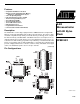
Features • Compatible with MCS-51™ Products • 8K Bytes of Reprogrammable Flash Memory • • • • • • • • • – Endurance: 1,000 Write/Erase Cycles 2.
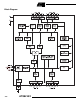
Block Diagram 4-84 AT89LV52
AT89LV52 The AT89LV52 provides the following standard features: 8K bytes of Flash, 256 bytes of RAM, 32 I/O lines, three 16bit timer/counters, a six-vector two-level interrupt architecture, a full duplex serial port, on-chip oscillator, and clock circuitry. In addition, the AT89LV52 is designed with static logic for operation down to zero frequency and supports two software selectable power saving modes.
pulse is skipped during each access to external data memory. If desired, ALE operation can be disabled by setting bit 0 of SFR location 8EH. With the bit set, ALE is active only during a MOVX or MOVC instruction. Otherwise, the pin is weakly pulled high. Setting the ALE-disable bit has no effect if the microcontroller is in external execution mode. PSEN Program Store Enable is the read strobe to external program memory.
AT89LV52 Special Function Registers A map of the on-chip memory area called the Special Function Register (SFR) space is shown in Table 1. Note that not all of the addresses are occupied, and unoccupied addresses may not be implemented on the chip. Read accesses to these addresses will in general return random data, and write accesses will have an indeterminate effect. User software should not write 1s to these unlisted locations, since they may be used in future products to invoke new features.
Timer 0 and 1 Timer 0 and Timer 1 in the AT89LV52 operate the same way as Timer 0 and Timer 1 in the AT89LV51. Timer 2 Timer 2 is a 16-bit Timer/Counter that can operate as either a timer or an event counter. The type of operation is selected by bit C/T2 in the SFR T2CON (shown in Table 2). Timer 2 has three operating modes: capture, auto-reload (up or down counting), and baud rate generator. The modes are selected by bits in T2CON, as shown in Table 3. Timer 2 consists of two 8-bit registers, TH2 and TL2.
AT89LV52 16-bit value in RCAP2H and RCAP2L. The values in RCAP2H and RCAP2L are preset by software. If EXEN2 = 1, a 16-bit reload can be triggered either by an overflow or by a 1-to-0 transition at external input T2EX. This transition also sets the EXF2 bit. Both the TF2 and EXF2 bits can generate an interrupt if enabled. Setting the DCEN bit enables Timer 2 to count up or down, as shown in Figure 3. In this mode, the T2EX pin controls the direction of the count. A logic 1 at T2EX makes Timer 2 count up.
Figure 3. Timer 2 Auto Reload Mode (DCEN = 1) (DOWN COUNTING RELOAD VALUE) 0FFH ÷12 OSC TOGGLE 0FFH EXF2 OVERFLOW C/T2 = 0 TH2 TL2 TF2 CONTROL TR2 C/T2 = 1 TIMER 2 INTERRUPT T2 PIN RCAP2H RCAP2L COUNT DIRECTION 1=UP 0=DOWN (UP COUNTING RELOAD VALUE) T2EX PIN Figure 4. Timer 2 in Baud Rate Generator Mode TIMER 1 OVERFLOW ÷2 "0" "1" NOTE: OSC. FREQ.
AT89LV52 Baud Rate Generator The baud rate formula is given below. Timer 2 is selected as the baud rate generator by setting TCLK and/or RCLK in T2CON (Table 2). Note that the baud rates for transmit and receive can be different if Timer 2 is used for the receiver or transmitter and Timer 1 is used for the other function. Setting RCLK and/or TCLK puts Timer 2 into its baud rate generator mode, as shown in Figure 4.
Programmable Clock Out A 50% duty cycle clock can be programmed to come out on P1.0, as shown in Figure 5. This pin, besides being a regular I/O pin, has two alternate functions. It can be programmed to input the external clock for Timer/Counter 2 or to output a 50% duty cycle clock ranging from 61 Hz to 3 MHz at a 12 MHz operating frequency. To configure the Timer/Counter 2 as a clock generator, bit C/T2 (T2CON.1) must be cleared and bit T2OE (T2MOD.1) must be set. Bit TR2 (T2CON.
AT89LV52 Oscillator Characteristics Figure 7. Oscillator Connections XTAL1 and XTAL2 are the input and output, respectively, of an inverting amplifier that can be configured for use as an on-chip oscillator, as shown in Figure 7. Either a quartz crystal or ceramic resonator may be used. To drive the device from an external clock source, XTAL2 should be left unconnected while XTAL1 is driven, as shown in Figure 8.
Program Memory Lock Bits The AT89LV52 has three lock bits that can be left unprogrammed (U) or can be programmed (P) to obtain the additional features listed in the following table: When lock bit 1 is programmed, the logic level at the EA pin is sampled and latched during reset. If the device is powered up without a reset, the latch initializes to a random value and holds that value until reset is activated.
AT89LV52 Ready/Busy: The progress of byte programming can also be monitored by the RDY/BSY output signal. P3.4 is pulled low after ALE goes high during programming to indicate BUSY. P3.4 is pulled high again when programming is done to indicate READY. Program Verify: If lock bits LB1 and LB2 have not been programmed, the programmed code data can be read back via the address and data lines for verification. The lock bits cannot be verified directly.
Figure 9. Programming the Flash Memory Figure 10. Verifying the Flash Memory VCC V CC Flash Programming and Verification Characteristics TA = 0°C to 70°C, VCC = 5.0 ± 10% Symbol VPP (1) Parameter Min Max Units Programming Enable Voltage 11.5 12.
AT89LV52 Flash Programming and Verification Waveforms (VPP = 12V) PROGRAMMING ADDRESS P1.0 - P1.7 P2.0 - P2.4 VERIFICATION ADDRESS tAVQV PORT 0 DATA IN tAVGL tDVGL tGHDX DATA OUT tGHAX ALE/PROG tSHGL tGLGH VPP tGHSL LOGIC 1 LOGIC 0 EA/VPP tEHSH tEHQZ tELQV P2.7 (ENABLE) tGHBL P3.
Absolute Maximum Ratings* Operating Temperature .................................. -55°C to +125°C *NOTICE: Storage Temperature ..................................... -65°C to +150°C Voltage on Any Pin with Respect to Ground .....................................-1.0V to +7.0V Maximum Operating Voltage............................................. 6.6V Stresses beyond those listed under “Absolute Maximum Ratings” may cause permanent damage to the device.
AT89LV52 AC Characteristics Under operating conditions, load capacitance for Port 0, ALE/PROG, and PSEN = 100 pF; load capacitance for all other outputs = 80 pF.
External Program Memory Read Cycle External Data Memory Read Cycle 4-100 AT89LV52
AT89LV52 External Data Memory Write Cycle External Clock Drive Waveforms External Clock Drive Symbol Parameter 1/tCLCL Oscillator Frequency tCLCL Clock Period tCHCX Min Max Units 0 12 MHz 83.
Serial Port Timing: Shift Register Mode Test Conditions The values in this table are valid for VCC = 2.7V to 6.0V and Load Capacitance = 80 pF. Symbol Parameter 12 MHz Osc Min Variable Oscillator Max Min Units Max tXLXL Serial Port Clock Cycle Time 1.
AT89LV52 AT89LV52 ICC (mA) TYPICAL ICC (ACTIVE) at 25o C 24 VCC = 6.0 V 20 16 VCC = 5.0 V 12 8 VCC = 3.0 V 4 0 0 4 8 12 16 20 24 F (MHz) AT89LV52 ICC (mA) TYPICAL ICC (IDLE) at 25 o C 4.8 VCC = 6.0 V 4.0 3.2 VCC = 5.0 V 2.4 1.6 VCC = 3.0 V 0.8 0.0 0 4 8 12 16 20 24 F (MHz) AT89LV52 TYPICAL ICC vs. VOLTAGE - POWER DOWN (85°C) 20 I 15 C C 10 µ A 5 0 3.0V 4.0V 5.0V 6.0V V CC VOLTAGE Notes: 1. XTAL1 tied to GND for Icc (power down) 2.
Ordering Information Speed (MHz) Power Supply 12 2.7V to 6V 12 Ordering Code 2.7V to 6V Package AT89LV52-12AC 44A Commercial AT89LV52-12JC 44J (0°C to 70°C) AT89LV52-12PC 40P6 AT89LV52-12AI 44A Industrial AT89LV52-12JI 44J (-40°C to 85°C) AT89LV52-12PI 40P6 Package Type 44A 44 Lead, Thin Plastic Gull Wing Quad Flatpack (TQFP) 44J 44 Lead, Plastic J-Leaded Chip Carrier (PLCC) 40P6 40 Lead, 0.