
User Manual


TL/H/11086
ADC08061/ADC08062
500 ns A/D Converter with S/H Function and Input Multiplexer
November 1995
ADC08061/ADC08062
500 ns A/D Converter with S/H Function
and Input Multiplexer
General Description
Using a patented multi-step A/D conversion technique, the
8-bit ADC08061 and ADC08062 CMOS ADCs offer 500 ns
(typ) conversion time, internal sample-and-hold (S/H), and
dissipate only 125 mW of power. The ADC08062 has a two-
channel multiplexer. The ADC08061/2 family performs an
8-bit conversion using a 2-bit voltage estimator that gener-
ates the 2 MSBs and two low-resolution (3-bit) flashes that
generate the 6 LSBs.
Input track-and-hold circuitry eliminates the need for an ex-
ternal sample-and-hold. The ADC08061/2 family performs
accurate conversions of full-scale input signals that have a
frequency range of DC to 300 kHz (full-power bandwidth)
without need of an external S/H.
The digital interface has been designed to ease connection
to microprocessors and allows the parts to be I/O or memo-
ry mapped.
Key Specifications
Y
Resolution 8 bits
Y
Conversion Time 560 ns max (WR-RD Mode)
Y
Full Power Bandwidth 300 kHz
Y
Throughput rate 1.5 MHz
Y
Power Dissipation 100 mW max
Y
Total Unadjusted Error
g
(/2 LSB and
g
1 LSB
Features
Y
1 or 2 input channels
Y
No external clock required
Y
Analog input voltage range from GND to V
a
Y
Overflow output available for cascading (ADC08061)
Y
ADC08061 pin-compatible with the industry standard
ADC0820
Applications
Y
Mobile telecommunications
Y
Hard disk drives
Y
Instrumentation
Y
High-speed data acquisition systems
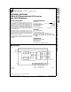
Block Diagram
*ADC08061 TL/H/11086–1
**ADC08062
TRI-STATE
É
is a registered trademark of National Semiconductor Corporation.
C
1996 National Semiconductor Corporation RRD-B30M36/Printed in U. S. A.
http://www.national.com