ADC081000 High Performance, Low Power 8-Bit, 1 GSPS A/D Converter General Description Features The ADC081000 is a low power, high performance CMOS analog-to-digital converter that digitizes signals to 8 bits resolution at sampling rates up to 1.6 GSPS. Consuming a typical 1.4 Watts at 1 GSPS from a single 1.9 Volt supply, this device is guaranteed to have no missing codes over the full operating temperature range.
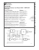
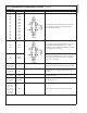
ADC081000 Ordering Information Extended Commercial Temperature Range (-40˚C < TA < +85˚C) NS Package ADC081000CIYB 128-Pin Exposed Pad LQFP ADC081000LEVAL Evaluation Board Pin Configuration 20068101 * Exposed pad on back of package must be soldered to ground plane to ensure rated performance. www.national.
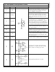
ADC081000 Pin Descriptions and Equivalent Circuits Pin Functions Pin No. Symbol Equivalent Circuit Description OutV Output Voltage Amplitude set. Tie this pin high for normal differential output amplitude. Ground this pin for a reduced differential output amplitude and reduced power consumption. See Section 1.5. OutEdge Output Edge Select. Sets the edge of the DCLK+ (pin 82) at which the output data transitions.
ADC081000 Pin Descriptions and Equivalent Circuits (Continued) Pin Functions Pin No. Symbol 7 VCMO Common Mode Output voltage for VIN+ and VIN- when d.c. input coupling is used. See Section 3.0. 31 VBG Bandgap output voltage. This pin is capable of sourcing or sinking up to 100 µA. 126 CalRun 32 REXT External Bias Resistor connection. The required value is 3.3k-Ohms ( ± 0.1%) to ground. See Section 1.1.
ADC081000 Pin Descriptions and Equivalent Circuits (Continued) Pin Functions Pin No. Symbol 104 105 106 107 111 112 113 114 115 116 117 118 122 123 124 125 Dd7Dd7+ Dd6Dd6+ Dd5Dd5+ Dd4Dd4+ Dd3Dd3+ Dd2Dd2+ Dd1Dd1+ Dd0Dd0+ Equivalent Circuit Description LVDS data output bits sampled first in time sequence. These outputs should always be terminated with a differential 100Ω resistance. 79 80 OR+ OR- Out of Range output.
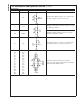
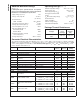
ADC081000 Absolute Maximum Ratings Operating Ratings (Notes 1, 2) (Notes 1, 2) Ambient Temperature Range If Military/Aerospace specified devices are required, please contact the National Semiconductor Sales Office/ Distributors for availability and specifications. Supply Voltage (VA) Supply Voltage (VA, VDR) 2.2V Voltage on Any Input Pin −0.15V to (VA +0.15V) Ground Difference |GND - DR GND| Package Input Current (Note 3) ± 25 mA ± 50 mA Power Dissipation at TA = 25˚C 2.
(Continued) The following specifications apply after calibration for VA = VDR = +1.9VDC, OutV = 1.9V, VIN FSR (a.c. coupled) = differential 800mVP-P, CL = 10 pF, Differential, a.c. coupled Sinewave Clock, fCLK = 1 GHz at 0.5VP-P with 50% duty cycle, REXT = 3300Ω ± 0.1%, Analog Signal Source Impedance = 100Ω. Boldface limits apply for TA = TMIN to TMAX. All other limits TA = 25˚C, unless otherwise stated.
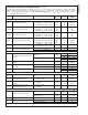
ADC081000 Converter Electrical Characteristics (Continued) The following specifications apply after calibration for VA = VDR = +1.9VDC, OutV = 1.9V, VIN FSR (a.c. coupled) = differential 800mVP-P, CL = 10 pF, Differential, a.c. coupled Sinewave Clock, fCLK = 1 GHz at 0.5VP-P with 50% duty cycle, REXT = 3300Ω ± 0.1%, Analog Signal Source Impedance = 100Ω. Boldface limits apply for TA = TMIN to TMAX. All other limits TA = 25˚C, unless otherwise stated.
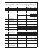
(Continued) The following specifications apply after calibration for VA = VDR = +1.9VDC, OutV = 1.9V, VIN FSR (a.c. coupled) = differential 800mVP-P, CL = 10 pF, Differential, a.c. coupled Sinewave Clock, fCLK = 1 GHz at 0.5VP-P with 50% duty cycle, REXT = 3300Ω ± 0.1%, Analog Signal Source Impedance = 100Ω. Boldface limits apply for TA = TMIN to TMAX. All other limits TA = 25˚C, unless otherwise stated.
ADC081000 Specification Definitions APERTURE (SAMPLING) DELAY is that time required after the fall of the clock input for the sampling switch to open. The Sample/Hold circuit effectively stops capturing the input signal and goes into the “hold” mode the aperture delay time (tAD) after the clock goes low. APERTURE JITTER (tAJ) is the variation in aperture delay from sample to sample. Aperture jitter shows up as input noise.
ADC081000 Specification Definitions (Continued) SIGNAL TO NOISE RATIO (SNR) is the ratio, expressed in dB, of the rms value of the input signal at the output to the rms value of the sum of all other spectral components below one-half the sampling frequency, not including harmonics or d.c. where Af1 is the RMS power of the fundamental (output) frequency and Af2 through Af10 are the RMS power of the first 9 harmonic frequencies in the output spectrum.
ADC081000 Transfer Characteristic 20068156 FIGURE 2. Input / Output Transfer Characteristic Timing Diagrams 20068114 FIGURE 3. ADC081000 Timing www.national.
INL INL vs. Temperature 20068117 20068118 INL vs. Supply Voltage INL vs. Output Driver Voltage 20068119 20068120 INL vs. Sample Rate DNL 20068121 20068122 13 www.national.com ADC081000 Typical Performance Characteristics VA = VDR = +1.9V, fCLK = 1 GHz (differential clock), fIN = 248 MHz, Differential Inputs, unless otherwise stated. Parameters shown across temperature were measured after recalibration at each temperature.
ADC081000 Typical Performance Characteristics VA = VDR = +1.9V, fCLK = 1 GHz (differential clock), fIN = 248 MHz, Differential Inputs, unless otherwise stated. Parameters shown across temperature were measured after recalibration at each temperature. (Continued) DNL vs. Temperature DNL vs. Supply Voltage 20068123 20068124 DNL vs. Output Driver Voltage DNL vs. Sample Rate 20068125 20068126 SNR vs. Temperature SNR vs. Supply Voltage 20068127 www.national.
SNR vs. Output Driver Voltage SNR vs. Sample Rate 20068129 20068130 SNR vs. Clock Duty Cycle SNR vs. Input Frequency 20068131 20068132 Distortion vs. Temperature Distortion vs. Supply Voltage 20068133 20068134 15 www.national.com ADC081000 Typical Performance Characteristics VA = VDR = +1.9V, fCLK = 1 GHz (differential clock), fIN = 248 MHz, Differential Inputs, unless otherwise stated. Parameters shown across temperature were measured after recalibration at each temperature.
ADC081000 Typical Performance Characteristics VA = VDR = +1.9V, fCLK = 1 GHz (differential clock), fIN = 248 MHz, Differential Inputs, unless otherwise stated. Parameters shown across temperature were measured after recalibration at each temperature. (Continued) Distortion vs. Sample Rate Distortion vs. Sample Rate 20068135 20068136 Distortion vs. Clock Duty Cycle Distortion vs. Input Frequency 20068137 20068138 Distortion vs. Input Common Mode SINAD vs. Temperature 20068181 www.national.
SINAD vs. Supply Voltage SINAD vs. Output Driver Voltage 20068140 20068141 SINAD vs. Sample Rate SINAD vs. Clock Duty Cycle 20068142 20068143 SINAD vs. Input Frequency ENOB vs. Temperature 20068160 20068161 17 www.national.com ADC081000 Typical Performance Characteristics VA = VDR = +1.9V, fCLK = 1 GHz (differential clock), fIN = 248 MHz, Differential Inputs, unless otherwise stated. Parameters shown across temperature were measured after recalibration at each temperature.
ADC081000 Typical Performance Characteristics VA = VDR = +1.9V, fCLK = 1 GHz (differential clock), fIN = 248 MHz, Differential Inputs, unless otherwise stated. Parameters shown across temperature were measured after recalibration at each temperature. (Continued) ENOB vs. Supply Voltage ENOB vs. Output Driver Voltage 20068162 20068163 ENOB vs. Sample Rate ENOB vs. Clock Duty Cycle 20068164 20068165 ENOB vs. Input Frequency ENOB vs. Input Common Mode 20068166 www.national.
SFDR vs. Temperature SFDR vs. Supply Voltage 20068167 20068168 SFDR vs. Output Driver Voltage SFDR vs. Sample Rate 20068169 20068170 SFDR vs. Clock Duty Cycle SFDR vs. Input Frequency 20068171 20068172 19 www.national.com ADC081000 Typical Performance Characteristics VA = VDR = +1.9V, fCLK = 1 GHz (differential clock), fIN = 248 MHz, Differential Inputs, unless otherwise stated. Parameters shown across temperature were measured after recalibration at each temperature.
ADC081000 Typical Performance Characteristics VA = VDR = +1.9V, fCLK = 1 GHz (differential clock), fIN = 248 MHz, Differential Inputs, unless otherwise stated. Parameters shown across temperature were measured after recalibration at each temperature. (Continued) Spectral Response @ fIN = 100 MHz Power Consumption vs. Sample Rate 20068174 20068175 Spectral Response @ fIN = 248 MHz Spectral Response @ fIN = 498 MHz 20068176 20068177 Spectral Response @ fIN = 1.5 GHz Spectral Response @ fIN = 1.
Intermodulation Distortion 20068183 21 www.national.com ADC081000 Typical Performance Characteristics VA = VDR = +1.9V, fCLK = 1 GHz (differential clock), fIN = 248 MHz, Differential Inputs, unless otherwise stated. Parameters shown across temperature were measured after recalibration at each temperature.
ADC081000 whenever the operating ambient temperature changes more than 30˚C since calibration was last performed. See Section 5.1.2 for more information. Functional Description The ADC081000 is a versatile, high performance, easy to use A/D Converter with an innovative architecture permitting very high speed operation. The controls available ease the application of the device to circuit solutions. The ADC081000 uses a calibrated folding and interpolating architecture that achieves over 7.5 effective bits.
TABLE 1. Digital Control Pins (Continued) PIN DESCRIPTION 1.4 Clocking The ADC081000 must be driven with an a.c. coupled, differential clock signal. Section 4 describes the use of the clock input pins. A differential LVDS output clock is available for use in latching the ADC output data into whatever receives that data. To help ease data capture, the output data may be caused to transition on either the positive or the negative edge of the output data clock (DCLK). This is chosen with the OutEdge input.
ADC081000 Applications Information (Continued) TABLE 3. DIFFERENTIAL INPUT TO OUTPUT RELATIONSHIP (FSR High) VIN+ VIN− Output Code VCM − 200 mV VCM + 200 mV 0000 0000 VCM − 99 mV VCM + 99 mV 0100 0000 VCM VCM 0111 1111 / 1000 0000 VCM + 101 mV VCM − 101 mV 1100 0000 VCM + 200mV VCM − 200 mV 1111 1111 20068155 Note that a precise d.c. common mode voltage must be present at the ADC inputs.
4.0 THE CLOCK INPUTS full-scale range of the ADC, "N" is the ADC resolution in bits and fIN is the maximum input frequency, in Hertz, to the ADC analog input. The ADC081000 has differential LVDS clock inputs, CLK+ and CLK-, which must be driven with an a.c. coupled, differential clock signal. Although the ADC081000 is tested and its performance is guaranteed with a differential 1.0 GHz clock, it typically will function well with clock frequencies indicated in the Electrical Characteristics Table.
ADC081000 Applications Information Since the minimum recommended clock rate for this device is 200 MSPS, the effective sample rate can be reduced to as low as 100 MSPS by using the results available on just one of the the two LVDS buses and a 200 MHz input clock, decimating the 200 MSPS data by two. There is one LVDS clock pair available for use to latch the LVDS outputs on both buses.
the exposed pad of the package and be located such that the exposed pad of the device is entirely over that thermal land pattern. This thermal land pattern should be electrically connected to ground. A clearance of at least 0.5 mm should separate this land pattern from the mounting pads for the package pins. Since a large aperture opening may result in poor release, the aperture opening should be subdivided into an array of smaller openings, similar to the land pattern of Figure 9.
ADC081000 Applications Information 10.0 COMMON APPLICATION PITFALLS (Continued) Allowing loose power supply voltage tolerance. The ADC081000 is specified for operation between 1.8 Volts to 2.0 Volts. Using a 1.8 Volt power supply then implies the need for no negative tolerance. The best solution is to use an adjustable linear regulator such as the LM317 or LM1086 set for 1.9V as discussed in Section 7.1. Driving the inputs (analog or digital) beyond the power supply rails.
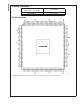
inches (millimeters) unless otherwise noted NOTES: UNLESS OTHERWISE SPECIFIED REFERENCE JEDEC REGISTRATION MS-026, VARIATION BFB. 128-Lead Exposed Pad LQFP Order Number ADC081000CIYB NS Package Number VNX128A LIFE SUPPORT POLICY NATIONAL’S PRODUCTS ARE NOT AUTHORIZED FOR USE AS CRITICAL COMPONENTS IN LIFE SUPPORT DEVICES OR SYSTEMS WITHOUT THE EXPRESS WRITTEN APPROVAL OF THE PRESIDENT AND GENERAL COUNSEL OF NATIONAL SEMICONDUCTOR CORPORATION. As used herein: 1.