
Instruction Manual

Functional Description (Continued)
4.0 THE ANALOG INPUTS
The most important feature of these converters is that they
can be located right at the analog signal source and through
just a few wires can communicate with a controlling proces-
sor with a highly noise immune serial bit stream. This in itself
greatly minimizes circuitry to maintain analog signal accura-
cy which otherwise is most susceptible to noise pickup.
However, a few words are in order with regard to the analog
inputs should the input be noisy to begin with or possibly
riding on a large common-mode voltage.
The differential input of these converters actually reduces
the effects of common-mode input noise, a signal common
to both selected ‘‘
a
’’ and ‘‘
b
’’ inputs for a conversion
(60 Hz is most typical). The time interval between sampling
the ‘‘
a
’’ input and then the ‘‘
b
’’ input is (/2 of a clock peri-
od. The change in the common-mode voltage during this
short time interval can cause conversion errors. For a sinus-
oidal common-mode signal this error is:
V
error
(max)
e
V
PEAK
(2qf
CM
)
#
0.5
f
CLK
J
where f
CM
is the frequency of the common-mode signal,
V
PEAK
is its peak voltage value
and f
CLK
is the A/D clock frequency.
For a 60Hz common-mode signal to generate a (/4 LSB er-
ror (
&
5mV) with the converter running at 250kHz, its peak
value would have to be 6.63V which would be larger than
allowed as it exceeds the maximum analog input limits.
Source resistance limitation is important with regard to the
DC leakage currents of the input multiplexer. While operat-
ing near or at maximum speed bypass capacitors should not
be used if the source resistance is greater than 1kX. The
worst-case leakage current of
g
1mA over temperature will
create a 1mV input error with a 1kX source resistance. An
op amp RC active low pass filter can provide both imped-
ance buffering and noise filtering should a high impedance
signal source be required.
5.0 OPTIONAL ADJUSTMENTS
5.1 Zero Error
The zero of the A/D does not require adjustment. If the
minimum analog input voltage value, V
IN(MIN)
, is not ground
a zero offset can be done. The converter can be made to
output 0000 0000 digital code for this minimum input voltage
by biasing any V
IN
(
b
) input at this V
IN(MIN)
value. This
utilizes the differential mode operation of the A/D.
The zero error of the A/D converter relates to the location
of the first riser of the transfer function and can be mea-
sured by grounding the V
IN
(
b
) input and applying a small
magnitude positive voltage to the V
IN
(
a
) input. Zero error
is the difference between the actual DC input voltage which
is necessary to just cause an output digital code transition
from 0000 0000 to 0000 0001 and the ideal (/2 LSB value
((/2 LSB
e
9.8mV for V
REF
e
5.000V
DC
).
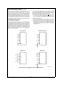
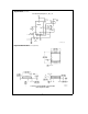
5.2 Full Scale
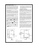
A full-scale adjustment can be made by applying a differen-
tial input voltage which is 1(/2 LSB down from the desired
analog full-scale voltage range and then adjusting the mag-
nitude of the V
REF
IN input for a digital output code which is
just changing from 1111 1110 to 1111 1111 (See figure enti-
tled ‘‘Span Adjust; 0V
s
V
IN
s
3V’’). This is possible only
with the ADC08134 and ADC08138. (The reference is inter-
nally connected to V
REF
IN of the ADC08131).
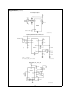
5.3 Adjusting for an Arbitrary Analog Input
Voltage Range
If the analog zero voltage of the A/D is shifted away from
ground (for example, to accommodate an analog input sig-
nal which does not go to ground), this new zero reference
should be properly adjusted first. A V
IN
(
a
) voltage which
equals this desired zero reference plus (/2 LSB (where the
LSB is calculated for the desired analog span, using 1 LSB
e
analog span/256) is applied to selected ‘‘
a
’’ input and
the zero reference voltage at the corresponding ‘‘
b
’’ input
should then be adjusted to just obtain the 00
HEX
to 01
HEX
code transition.
The full-scale adjustment should be made
[
with the proper
V
IN
(
b
) voltage applied
]
by forcing a voltage to the V
IN
(
a
)
input which is given by:
V
IN
(
a
)fsadj
e
V
MAX
b
1.5
Ð
(V
MAX
b
V
MIN
)
256
(
where:
V
MAX
e
the high end of the analog input range
and
V
MIN
e
the low end (the offset zero) of the analog range.
(Both are ground referenced.)
The V
REF
IN (or V
CC
) voltage is then adjusted to provide a
code change from FE
HEX
to FF
HEX
. This completes the ad-
justment procedure.
16