
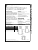
Instruction Manual
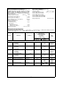
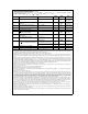


Absolute Maximum Ratings (Notes1&3)
If Military/Aerospace specified devices are required,
please contact the National Semiconductor Sales
Office/Distributors for availability and specifications.
Supply Voltage (V
CC
) 6.5V
Voltage at Inputs and Outputs
b
0.3V to V
CC
a
0.3V
Input Current at Any Pin (Note 4)
g
5mA
Package Input Current (Note 4)
g
20 mA
Power Dissipation at T
A
e
25
§
C (Note 5) 800 mW
ESD Susceptibility (Note 6) 1500V
Soldering Information
N Package (10 sec.) 260
§
C
SO Package:
Vapor Phase (60 sec.) 215
§
C
Infrared (15 sec.) (Note 7) 220
§
C
Storage Temperature
b
65
§
Cto
a
150
§
C
Operating Ratings (Notes2&3)
Temperature Range T
MIN
s
T
A
s
T
MAX
ADC08131BIN, ADC08131CIN,
b
40
§
C
s
T
A
s
a
85
§
C
ADC08134BIN, ADC08134CIN,
ADC08138BIN, ADC08138CIN,
ADC08134BIWM, ADC08138BIWM,
ADC08134CIWM, ADC08138CIWM
Supply Voltage (V
CC
) 4.5 V
DC
to 6.3 V
DC
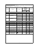
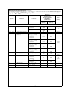
Electrical Characteristics
The following specifications apply for V
CC
ea
5V
DC
,V
REF
ea
2.5 V
DC
and f
CLK
e
1 MHz unless otherwise specified.
Boldface limits apply for T
A
e
T
J
e
T
MIN
to T
MAX
; all other limits T
A
e
T
J
e
25
§
C.
ADC08131,
ADC08134 and
ADC08138 with BIN,
Units
Symbol Parameter Conditions CIN, BIWM or
(Limits)
CIWM Suffixes
Typical Limits
(Note 8) (Note 9)
CONVERTER AND MULTIPLEXER CHARACTERISTICS
Linearity Error V
REF
ea
2.5 V
DC
BIN, BIWM
g
(/2 LSB (max)
CIN, CIWM
g
1 LSB (max)
Full Scale Error V
REF
ea
2.5 V
DC
BIN, BIWM
g
(/2 LSB (max)
CIN, CIWM
g
1 LSB (max)
Zero Error V
REF
ea
2.5 V
DC
BIN, BIWM
g
1 LSB (max)
CIN, CIWM
g
1 LSB (max)
Total Unadjusted Error V
REF
ea
5V
DC
BIN, BIWM (Note 10)
g
(/2 LSB (max)
CIN, CIWM
g
1 LSB (max)
Differential Linearity V
REF
ea
2.5 V
DC
8 Bits (min)
R
REF
Reference Input Resistance (Note 11) 3.5 kX
1.3 kX (min)
6.0 kX (max)
V
IN
Analog Input Voltage (Note 12) (V
CC
a
0.05) V (max)
(GND
b
0.05) V (min)
2