
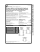
Instruction Manual
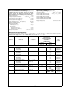

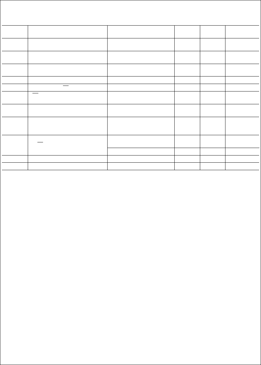
Electrical Characteristics (Continued)
The following specifications apply for V
CC
ea
5V
DC
,V
REF
ea
2.5 V
DC
and t
r
e
t
f
e
20 ns unless otherwise specified.
Boldface limits apply for T
A
e
T
J
e
T
MIN
to T
MAX
; all other limits T
A
e
T
J
e
25
§
C.
Symbol Parameter Conditions
Typical Limits Units
(Note 8) (Note 9) (Limits)
f
CLK
Clock Frequency 10 kHz (min)
1 MHz (max)
Clock Duty Cycle 40 % (min)
(Note 14) 60 % (max)
T
C
Conversion Time (Not Including f
CLK
e
1 MHz 8 1/f
CLK
(max)
MUX Addressing Time) 8 ms (max)
t
CA
Acquisition Time (/2 1/f
CLK
(max)
t
SELECT
CLK High while CS is High 50 ns
t
SET-UP
CS Falling Edge or Data Input
25 ns (min)
Valid to CLK Rising Edge
t
HOLD
Data Input Valid after CLK
20 ns (min)
Rising Edge
t
pd1
,t
pd0
CLK Falling Edge to Output C
L
e
100 pF:
Data Valid (Note 15) Data MSB First 250 ns (max)
Data LSB First 200 ns (max)
t
1H
,t
0H
TRI-STATE Delay from Rising Edge C
L
e
10 pF, R
L
e
10 kX
50 ns
of CS
to Data Output and SARS Hi-Z (see TRI-STATE Test Circuits)
C
L
e
100 pF, R
L
e
2kX 180 ns (max)
C
IN
Capacitance of Logic Inputs 5 pF
C
OUT
Capacitance of Logic Outputs 5 pF
Note 1: Absolute Maximum Ratings indicate limits beyond which damage to the device may occur.
Note 2: Operating Ratings indicate conditions for which the device is functional. These ratings do not guarantee specific performance limits. For guaranteed
specifications and test conditions, see the Electrical Characteristics. The guaranteed specifications apply only for the test conditions listed. Some performance
characteristics may degrade when the device is not operated under the listed test conditions.
Note 3: All voltages are measured with respect to AGND
e
DGND
e
0V
DC
, unless otherwise specified.
Note 4: When the input voltage (V
IN
) at any pin exceeds the power supplies (V
IN
k
(AGND or DGND) or V
IN
l
AV
CC
,) the current at that pin should be limited to
5 mA. The 20 mA maximum package input current rating limits the number of pins that can safely exceed the power supplies with an input current of 5 mA to four
pins.
Note 5: The maximum power dissipation must be derated at elevated temperatures and is dictated by T
J
MAX
, i
JA
and the ambient temperature, T
A
. The maximum
allowable power dissipation at any temperature is P
D
e
(T
J
MAX
b
T
A
)/i
JA
or the number given in the Absolute Maximum Ratings, whichever is lower. For devices
with suffixes BIN, CIN, BIJ, CIJ, BIWM, and CIWM T
J
MAX
e
125
§
C. For devices with suffix CMJ, T
J
MAX
e
150
§
C. The typical thermal resistances (i
JA
) of these
parts when board mounted follow: ADC08131 with BIN and CIN suffixes 120
§
C/W, ADC08134 with BIN and CIN suffixes 95
§
C/W, ADC08138 with BIN and CIN
suffixes 80
§
C/W. ADC08134 with BIWM and CIWM suffixes 140
§
C/W, ADC08138 with BIWM and CIWM suffixes 91
§
C/W,
Note 6: Human body model, 100 pF capacitor discharged through a 1.5 kX resistor.
Note 7: See AN450 ‘‘Surface Mounting Methods and Their Effect on Product Reliability’’ or
Linear Data Book
section ‘‘Surface Mount’’ for other methods of
soldering surface mount devices.
Note 8: Typicals are at T
J
e
25
§
C and represent the most likely parametric norm.
Note 9: Guaranteed to National’s AOQL (Average Outgoing Quality Level).
Note 10: Total unadjusted error includes zero, full-scale, linearity, and multiplexer error. Total unadjusted error with V
REF
ea
5V only applies to the ADC08134
and ADC08138. See Note 16.
Note 11: Cannot be tested for the ADC08131.
Note 12: For V
IN(
b
)
t
V
IN(
a
)
the digital code will be 0000 0000. Two on-chip diodes are tied to each analog input (see Block Diagram) which will forward-conduct
for analog input voltages one diode drop below ground or one diode drop greater than V
CC
supply. During testing at low V
CC
levels (e.g., 4.5V), high level analog
inputs (e.g., 5V) can cause an input diode to conduct, especially at elevated temperatures. This will cause errors for analog inputs near full-scale. The specification
allows 50 mV forward bias of either diode; this means that as long as the analog V
IN
does not exceed the supply voltage by more than 50 mV, the output code will
be correct. Exceeding this range on an unselected channel will corrupt the reading of a selected channel. Achievement of an absolute 0 V
DC
to5V
DC
input voltage
range will therefore require a minimum supply voltage of 4.950 V
DC
over temperature variations, initial tolerance and loading.
Note 13: Channel leakage current is measured after a single-ended channel is selected and the clock is turned off. For off channel leakage current the following
two cases are considered: one, with the selected channel tied high (5 V
DC
) and the remaining seven off channels tied low (0 V
DC
), total current flow through the off
channels is measured; two, with the selected channel tied low and the off channels tied high, total current flow through the off channels is again measured. The two
cases considered for determining on channel leakage current are the same except total current flow through the selected channel is measured.
Note 14: A 40% to 60% duty cycle range insures proper operation at all clock frequencies. In the case that an available clock has a duty cycle outside of these
limits the minimum time the clock is high or low must be at least 450 ns. The maximum time the clock can be high or low is 100 ms.
Note 15: Since data, MSB first, is the output of the comparator used in the successive approximation loop, an additional delay is built in (see Block Diagram) to
allow for comparator response time.
Note 16: For the ADC08131 V
REF
IN is internally tied to the on chip 2.5V band-gap reference output; therefore, the supply current is larger because it includes the
reference current (700 mA typical, 2 mA maximum).
Note 17: Load regulation test conditions and specifications for the ADC08131 differ from those of the ADC08134 and ADC08138 because the ADC08131 has the
on-board reference as a permanent load.
5