
Owner manual


1.0 Functional Description (Continued)
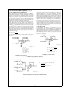
When a typical conversion is started, the WR
line is brought
low. At this instant the MS comparators go from zeroing to
comparison mode (
Figure 8
). When WR is returned high af-
ter at least 600 ns, the output from the first set of compara-
tors (the first flash) is decoded and latched. At this point the
two 4-bit converters change modes and the LS (least signifi-
cant) flash ADC enters its compare cycle. No less than 600
ns later, the RD
line may be pulled low to latch the lower 4
data bits and finish the 8-bit conversion. When RD
goes low,
the flash A/Ds change state once again in preparation for
the next conversion.
Figure 8
also outlines how the converter’s interface timing
relates to its analog input (V
IN
). In WR-RD mode, V
IN
is
measured while WR
is low. In RD mode, sampling occurs
during the first 800 ns of RD
. Because of the input connec-
tions to the ADC0820’s LS and MS comparators, the con-
verter has the ability to sample V
IN
at one instant (Section
2.4), despite the fact that two separate 4-bit conversions are
being done. More specifically, when WR
is low the MS flash
is in compare mode (connected to V
IN
), and the LS flash is
in zero mode (also connected to V
IN
). Therefore both flash
ADCs sample V
IN
at the same time.
1.4 DIGITAL INTERFACE
The ADC0820 has two basic interface modes which are se-
lected by strapping the MODE pin high or low.
RD Mode
With the MODE pin grounded, the converter is set to Read
mode. In this configuration, a complete conversion is done
by pulling RD
low until output data appears. An INT line is
provided which goes low at the end of the conversion as
well as a RDY output which can be used to signal a proces-
sor that the converter is busy or can also serve as a system
Transfer Acknowledge signal.
RD Mode (Pin 7 is Low)
TL/H/5501–16
When in RD mode, the comparator phases are internally
triggered. At the falling edge of RD
, the MS flash converter
goes from zero to compare mode and the LS ADC’s com-
parators enter their zero cycle. After 800 ns, data from the
MS flash is latched and the LS flash ADC enters compare
mode. Following another 800 ns, the lower 4 bits are recov-
ered.
WR then RD Mode
With the MODE pin tied high, the A/D will be set up for the
WR-RD mode. Here, a conversion is started with the WR
input; however, there are two options for reading the output
data which relate to interface timing. If an interrupt driven
scheme is desired, the user can wait for INT
to go low be-
fore reading the conversion result (
Figure B
). INT will typi-
cally go low 800 ns after WR
’s rising edge. However, if a
shorter conversion time is desired, the processor need not
wait for INT
and can exercise a read after only 600 ns (
Fig-
ure A
). If this is done, INT will immediately go low and data
will appear at the outputs.
TL/H/5501–17
FIGURE A. WR-RD Mode (Pin 7 is High and t
RD
k
t
I
)
TL/H/5501–18
FIGURE B. WR-RD Mode (Pin 7 is High and t
RD
l
t
I
)
Stand-Alone
For stand-alone operation in WR-RD mode, CS
and RD can
be tied low and a conversion can be started with WR
. Data
will be valid approximately 800 ns following WR
’s rising
edge.
WR-RD Mode (Pin 7 is High) Stand-Alone Operation
TL/H/5501–19
10