January 2005 ADC08D1000 High Performance, Low Power, Dual 8-Bit, 1 GSPS A/D Converter General Description Features NOTE: This product is currently in development. – ALL specifications are design targets and are subject to change. n n n n n n n n n The ADC08D1000 is a dual, low power, high performance CMOS analog-to-digital converter that digitizes signals to 8 bits resolution at sampling rates up to 1.3 GSPS. Consuming a typical 1.6 Watts at 1 GSPS from a single 1.
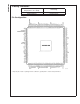
ADC08D1000 Ordering Information Extended Commercial Temperature Range (-40˚C < TA < +85˚C) NS Package ADC08D1000CIYB 128-Pin Exposed Pad LQFP ADC08D1000EVAL Evaluation Board Pin Configuration 20097401 * Exposed pad on back of package must be soldered to ground plane to ensure rated performance. www.national.
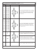
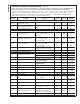
Pin Functions Pin No. Symbol Equivalent Circuit Description OutV / SCLK Output Voltage Amplitude and Serial Interface Clock. Tie this pin high for normal differential DCLK and data amplitude. Ground this pin for a reduced differential output amplitude and reduced power consumption. See Section 1.1.6. When the extended control mode is enabled, this pin functions as the SCLK input which clocks in the serial data. See Section 1.
ADC08D1000 Pin Descriptions and Equivalent Circuits (Continued) Pin Functions Pin No. Symbol 18 19 CLK+ CLK- LVDS Clock input pins for the ADC. The differential clock signal must be a.c. coupled to these pins. The input signal is sampled on the falling edge of CLK+. See Section 2.3. 11 10 . 22 23 VINI+ VINI− . VINQ+ VINQ− Analog signal inputs to the ADC. The differential full-scale input range is 650 mVP-P when the FSR pin is low, or 860 mVP-P when the FSR pin is high.
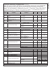
ADC08D1000 Pin Descriptions and Equivalent Circuits (Continued) Pin Functions Pin No.
ADC08D1000 Pin Descriptions and Equivalent Circuits (Continued) Pin Functions Pin No. Symbol 40, 51 ,62, 73, 88, 99, 110, 121 VDR Output Driver power supply pins. Bypass these pins to DR GND. 1, 6, 9, 12, 21, 24, 27, 41 GND Ground return for VA. 42, 53, 64, 74, 87, 97, 108, 119 DR GND 52, 63, 98, 109, 120 NC www.national.com Equivalent Circuit Description Ground return for VDR. No Connection. Make no connection to these pins.
Operating Ratings (Notes 1, 2) (Notes 1, 2) Ambient Temperature Range If Military/Aerospace specified devices are required, please contact the National Semiconductor Sales Office/ Distributors for availability and specifications. Supply Voltage (VA) Supply Voltage (VA, VDR) 2.2V Voltage on Any Input Pin −0.15V to (VA +0.15V) Ground Difference |GND - DR GND| Package Input Current (Note 3) ± 25 mA ± 50 mA Power Dissipation at TA = 25˚C 2.
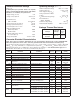
ADC08D1000 Converter Electrical Characteristics (Continued) [Note: This product is currently in development. As such, the parameters specified in this section are DESIGN TARGETS. The specifications in this section cannot be guaranteed until device characterization has taken place.] The following specifications apply after calibration for VA = VDR = +1.9VDC, OutV = 1.9V, VIN FSR (a.c. coupled) = differential 860mVP-P, CL = 10 pF, Differential, a.c. coupled Sinewave Input Clock, fCLK = 1 GHz at 0.
(Continued) [Note: This product is currently in development. As such, the parameters specified in this section are DESIGN TARGETS. The specifications in this section cannot be guaranteed until device characterization has taken place.] The following specifications apply after calibration for VA = VDR = +1.9VDC, OutV = 1.9V, VIN FSR (a.c. coupled) = differential 860mVP-P, CL = 10 pF, Differential, a.c. coupled Sinewave Input Clock, fCLK = 1 GHz at 0.
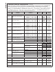
ADC08D1000 Converter Electrical Characteristics (Continued) 20097404 Note 7: To guarantee accuracy, it is required that VA and VDR be well bypassed. Each supply pin must be decoupled with separate bypass capacitors. Additionally, achieving rated performance requires that the backside exposed pad be well grounded. Note 8: Typical figures are at TJ = 25˚C, and represent most likely parametric norms. Test limits are guaranteed to National’s AOQL (Average Outgoing Quality Level).
ADC08D1000 Specification Definitions APERTURE (SAMPLING) DELAY is that time required after the fall of the clock input for the sampling switch to open. The Sample/Hold circuit effectively stops capturing the input signal and goes into the “hold” mode the aperture delay time (tAD) after the input clock goes low. APERTURE JITTER (tAJ) is the variation in aperture delay from sample to sample. Aperture jitter shows up as input noise. Bit Error Rate (B.E.R.
ADC08D1000 Specification Definitions (Continued) SIGNAL TO NOISE RATIO (SNR) is the ratio, expressed in dB, of the rms value of the input signal at the output to the rms value of the sum of all other spectral components below one-half the sampling frequency, not including harmonics or d.c. where Af1 is the RMS power of the fundamental (output) frequency and Af2 through Af10 are the RMS power of the first 9 harmonic frequencies in the output spectrum.
ADC08D1000 Timing Diagrams 20097414 FIGURE 3. ADC08D1000 Timing — SDR Clocking 20097415 FIGURE 4. ADC08D1000 Timing — DDR Clocking 15 www.national.
ADC08D1000 Timing Diagrams (Continued) 20097419 FIGURE 5. Serial Interface Timing 20097420 FIGURE 6. Clock Reset Timing in DDR Mode 20097423 FIGURE 7. Clock Reset Timing in SDR Mode with OUTEDGE Low www.national.
ADC08D1000 Timing Diagrams (Continued) 20097424 FIGURE 8. Clock Reset Timing in SDR Mode with OUTEDGE High 20097425 FIGURE 9. Self Calibration and On-Command Calibration Timing 17 www.national.
ADC08D1000 tion can not be initiated or run while the device is in the power-down mode. See Section 1.1.7 for information on the interaction between Power Down and Calibration. 1.0 Functional Description The ADC08D1000 is a versatile A/D Converter with an innovative architecture permitting very high speed operation. The controls available ease the application of the device to circuit solutions.
The ADC08D1000 also has the option to use a duty cycle corrected clock receiver as part of the input clock circuit. This feature is enabled by default and provides improved ADC clocking especially in the Dual-Edge Sampling mode (DES). This circuitry allows the ADC to be clocked with a signal source having a duty cycle ratio of 80 / 20 % (worst case) for both the normal and the Dual Edge Sampling modes. (Continued) controls are disabled.
ADC08D1000 1.0 Functional Description If the PD input is brought high while a calibration is running, the device will not go into power down until the calibration sequence is complete. However, if power is applied and PD is already high, the device will not begin the calibration sequence until the PD input goes low. If a manual calibration is requested while the device is powered down, the calibration will not begin at all.
TABLE 4. Register Addresses (Continued) 4-Bit Address The default state of the Extended Control Mode is set upon power-on reset (internally performed by the device) and is shown in Table 3. Loading Sequence: A3 loaded after H0, A0 loaded last TABLE 3. Extended Control Mode Operation (Pin 14 Floating) Feature ADC08D1000 1.
ADC08D1000 1.0 Functional Description Bit 10 I-Channel Full-Scale Voltage Adjust (Continued) Addr: 3h (0011b) nDE: DDR Enable. When this bit is set to 0b, data bus clocking follows the DDR (Dual Data Rate) mode whereby a data word is output with each rising and falling edge of DCLK. When this bit is set to a 1b, data bus clocking follows the SDR (single data rate) mode whereby each data word is output with either the rising or falling edge of DCLK , as determined by the OutEdge bit.
(Continued) Bit 14 Automatic Clock Phase Control. Setting this bit to 1b enables the Automatic Clock Phase Control. In this mode the DES Coarse and Fine manual controls are disabled. A phase detection circuit continually adjusts the I and Q sampling edges to be 180 degrees out of phase. When this bit is set to 1b, the sample (input) clock delay between the I and Q channels is set manually using the DES Coarse and Fine Adjust registers. (See Section 2.4.
ADC08D1000 1.0 Functional Description and hold times with respect to the CLK input rising edge. These times are specified in the AC Electrical Characteristics Table. The DCLK_RST signal can be asserted asynchronous to the input clock. If DCLK_RST is asserted, the DCLK output is immediately held in a designated state. The state in which DCLK is held during the reset period is determined by the mode of operation (SDR/DDR) and the setting of the Output Edge configuration pin or bit.
If d.c. coupling is used, it is best to servo the input common mode voltage, using the VCMO pin, to maintain optimum performance. An example of this type of circuit is shown in Figure 12. (Continued) reduced to 75% of the values indicated. In the Enhanced Control Mode, these values will be determined by the full scale range and offset settings in the Control Registers. TABLE 5.
ADC08D1000 2.0 Applications Information The low and high times of the input clock signal can affect the performance of any A/D Converter. The ADC08D1000 features a duty cycle clock correction circuit which can maintain performance over temperature even in DES mode. The ADC will meet its performance specification if the input clock high and low times are maintained within the range (20/80% ratio) as specified in the Electrical Characteristics Table. (Continued) 2.2.
rising edge or the falling edge of the DCLK signal, so that either edge of that DCLK signal can be used to latch the output data into the receiving circuit. When OutEdge (pin 4) is high, the output data is synchronized with (changes with) the rising edge of the DCLK+ (pin 82). When OutEdge is low, the output data is synchronized with the falling edge of DCLK+.
ADC08D1000 2.0 Applications Information The VA and VDR supply pins should be isolated from each other to prevent any digital noise from being coupled into the analog portions of the ADC. A ferrite choke, such as the JW Miller FB20009-3B, is recommended between these supply lines when a common source is used for them. As is the case with all high speed converters, the ADC08D1000 should be assumed to have little power supply noise rejection.
To minimize junction temperature, it is recommended that a simple heat sink be built into the PCB. This is done by including a copper area of about 2 square inches (6.5 square cm) on the opposite side of the PCB. This copper area may be plated or solder coated to prevent corrosion, but should not have a conformal coating, which could provide some thermal insulation. Thermal vias should be used to connect these top and bottom copper areas.
ADC08D1000 2.0 Applications Information this pin is floating, the output clock (DCLK) is a DDR (Double Data Rate) clock (see Section 1.1.5.3) and the output edge synchronization is irrelevant since data is clocked out on both DCLK edges. Pin 127, if it is high or low in the non-extended control mode, sets the calibration delay. If pin 127 is floating, the calibration delay is the same as it would be with this pin low and the converter performs dual edge sampling (DES). (Continued) ADC08D1000.
moval to ensure device reliability. This can either be done with adequate air flow or the use of a simple heat sink built into the board. The backside pad should be grounded for best performance. (Continued) Failure to provide adequate heat removal. As described in Section 2.6.2, it is important to provide adequate heat re- 31 www.national.com ADC08D1000 2.
High Performance, Low Power, Dual 8-Bit, 1 GSPS A/D Converter Physical Dimensions inches (millimeters) unless otherwise noted NOTES: UNLESS OTHERWISE SPECIFIED REFERENCE JEDEC REGISTRATION MS-026, VARIATION BFB.