
Instruction Manual
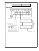
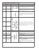
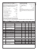
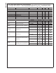

Pin Descriptions and Equivalent Circuits
Pin No. Symbol Equivalent Circuit Description
ANALOG I/O
12 V
IN
−
Inverting analog input signal. With a 1.2V reference the
full-scale input signal level is 1.0 V
P-P
. This pin may be tied to
V
COM
(pin 4) for single-ended operation.
13 V
IN
+
Non-inverting analog input signal. With a 1.2V reference the
full-scale input signal level is 1.0 V
P-P
.
6V
REF
Reference input. This pin should be bypassed to V
SSA
with a
0.1 µF monolithic capacitor. V
REF
is 1.20V nominal. This pin
may be driven by a 1.20V external reference if desired. Do
not load this pin.
7V
REFT
V
REFT
and V
REFB
are high impedance reference bypass pins
only. Connect a 0.1 µF capacitor from each of these pins to
V
SSA
. These pins should not be loaded. V
COM
should also be
bypassed with a 0.1 µF capacitor to V
SSA
.V
COM
may be used
to set the input common voltage V
CM
.
4V
COM
8V
REFB
DIGITAL I/O
1 CLK
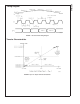
Digital clock input. The range of frequencies for this input is
20 MHz to 80 MHz. The input is sampled on the rising edge
of this input.
15 DF
DF = “1” Two’s Complement
DF = “0” Offset Binary
28 STBY
This is the standby pin. When high, this pin sets the converter
into standby mode. When this pin is low, the converter is in
active mode.
5
IRS (Input Range
Select)
IRS=“V
DDA
” 2.0 V
P-P
input range
IRS=“V
SSA
” 1.5 V
P-P
input range
IRS = “Floating” 1.0 V
P-P
input range
If using both V
IN
+ and V
IN
- pins, (or differential mode), then
the peak-to-peak voltage refers to the differential voltage
(V
IN
+-V
IN
-).
ADC10080
www.national.com3