
Instruction Manual
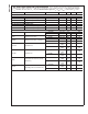

Absolute Maximum Ratings (Notes 1,
2)
If Military/Aerospace specified devices are required,
please contact the National Semiconductor Sales Office/
Distributors for availability and specifications.
V
DDA
,V
DDIO
3.9V
Voltage on Any Pin to GND −0.3V to V
DDA
or
V
DDIO
+0.3V
Input Current on Any Pin
±
25 mA
Package Input Current (Note 3)
±
50 mA
Package Dissipation at T = 25˚C See (Note 4)
ESD Susceptibility
Human Body Model (Note 5) 2500V
Machine Model (Note 5) 250V
Soldering Temperature
Infrared, 10 sec. (Note 6) 235˚C
Storage Temperature −65˚C to +150˚C
Operating Ratings
Operating Temperature Range −40˚C ≤ T
A
≤ +85˚C
V
DDA
(Supply Voltage) +2.7V to +3.6V
V
DDIO
(Output Driver Supply
Voltage) +2.5V to V
DDA
V
REF
1.20V
|V
SSA
–V
SSIO
| ≤ 100 mV
NOTE: Absolute maximum ratings are limiting values, to be applied individu-
ally, and beyond which the serviceability of the circuit may be impaired.
Functional operability under any of these conditions is not necessarily im-
plied. Exposure to maximum ratings for extended periods may affect device
reliability.
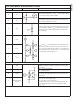
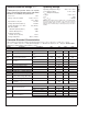
Converter Electrical Characteristics
Unless otherwise specified, the following specifications apply for V
SSA
=V
SSIO
= 0V, V
DDA
= +3.0V, V
DDIO
= +2.5V,
V
IN
=2V
P-P
, STBY = 0V, V
REF
= 1.20V, (External Supply) f
CLK
= 80 MHz, 50% Duty Cycle, C
L
= 10 pF/pin. Boldface limits
apply for T
A
=T
MIN
to T
MAX
: all other limits T
A
= 25˚C.
Symbol Parameter Conditions Min Typ Max Units
STATIC CONVERTER CHARACTERISTICS
No Missing Codes Guaranteed 10 Bits
INL Integral Non-Linearity (Note 11)
F
IN
= 500 kHz, 0 dB Full
Scale
−1.4
±
0.5 +1.6 LSB
DNL Differential Non-Linearity
F
IN
= 500 kHz, 0 dB Full
Scale
−0.9
±
0.25 +1.0 LSB
GE Gain Error
Positive Error −1.6 +0.5% +2.0 %FS
Negative Error −1.6 −0.07% +2.0 %FS
OE Offset Error (V
IN
+=V
IN
−) −1.4 0.11 1.7 %FS
Under Range Output Code 0
Over Range Output Code 1023
FPBW Full Power Bandwidth 400 MHz
REFERENCE AND INPUT CHARACTERISTICS
V
CM
Common Mode Input Voltage 0.5 1.5 V
V
COM
Output Voltage for use as an input
common mode voltage (Note 16)
1.45
V
V
REF
Reference Voltage 1.2 V
V
REFTC
Reference Voltage Temperature
Coefficient
±
80 ppm/˚C
POWER SUPPLY CHARACTERISTICS
I
VDDA
Analog Supply Current
STBY = 1 5 6.3 mA
STBY 0 25 32 mA
I
VDDIO
Digital Supply Current
STBY=1,f
IN
=0Hz 0 mA
STBY 0, f
IN
=0Hz 1.2 1.4 mA
PWR Power Consumption
STBY = 1 15 18.9 mW
STBY = 0 78.6 100.2 mW
ADC10080
www.national.com5