
Manual
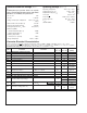

Pin Descriptions and Equivalent Circuits (Continued)
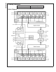
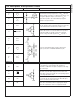
Pin No. Symbol Equivalent Circuit Description
25–29
34–39
DA0–DA10
Digital data output pins that make up the 11-bit conversion
results of their respective converters. DA0 and DB0 are the
LSBs, while DA10 and DB10 are the MSBs of the output
words. Output levels are TTL/CMOS compatible.
43–47
52–57
DB0–DB10
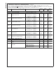
ANALOG POWER
9, 18, 19,
62, 63
V
A
Positive analog supply pins. These pins should be connected
to a quiet +3.3V source and bypassed to AGND with 0.1 µF
capacitors located within 1 cm of these power pins, and with
a 10 µF capacitor.
3, 8, 10, 17,
20, 61, 64
AGND The ground return for the analog supply.
DIGITAL POWER
33, 48 V
D
Positive digital supply pin. This pin should be connected to
the same quiet +3.3V source as is V
A
and be bypassed to
DGND with a 0.1 µF capacitor located within 1 cm of the
power pin and with a 10 µF capacitor.
32, 49 DGND The ground return for the digital supply.
24, 42 DGND
These two pins are grounded internally and may be
grounded or left unconnected.
30, 51 V
DR
Positive digital supply pin for the ADC11DL066’s output
drivers. This pin should be connected to a voltage source of
+2.4V to V
D
and be bypassed to DR GND with a 0.1 µF
capacitor. If the supply for this pin is different from the
supply used for V
A
and V
D
, it should also be bypassed with
a 10 µF tantalum capacitor. V
DR
should never exceed the
voltage on V
D
. All bypass capacitors should be located
within 1 cm of the supply pin.
23, 31, 40,
50, 58
DR GND
The ground return for the digital supply for the
ADC11DL066’s output drivers. These pins should be
connected to the system digital ground, but not be
connected in close proximity to the ADC11DL066’s DGND or
AGND pins. See Section 5 (Layout and Grounding) for more
details.
ADC11DL066
www.national.com 4