
Manual
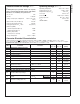

Absolute Maximum Ratings (Notes 1,
2)
If Military/Aerospace specified devices are required,
please contact the National Semiconductor Sales Office/
Distributors for availability and specifications.
V
A
,V
D
,V
DR
4.2V
|V
A
–V
D
| ≤ 100 mV
Voltage on Any Input or Output Pin −0.3V to (V
A
or V
D
+0.3V)
Input Current at Any Pin (Note 3)
±
25 mA
Package Input Current (Note 3)
±
50 mA
Package Dissipation at T
A
= 25˚C See (Note 4)
ESD Susceptibility
Human Body Model (Note 5) 2500V
Machine Model (Note 5) 250V
Soldering Temperature,
Infrared, 10 sec. (Note 6) 235˚C
Storage Temperature −65˚C to +150˚C
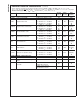
Operating Ratings (Notes 1, 2)
Operating Temperature −40˚C ≤ T
A
≤ +85˚C
Supply Voltage (V
A
,V
D
) +3.0V to +3.6V
Output Driver Supply (V
DR
) +2.4V to V
D
V
REF
Input 0.8V to 1.5V
CLK, PD, OE
−0.05V to (V
D
+ 0.05V)
Analog Input Pins 0V to (V
A
− 0.5V)
V
CM
0.5V to 1.8V
|AGND–DGND| ≤100mV
Converter Electrical Characteristics
Unless otherwise specified, the following specifications apply for AGND = DGND = DR GND = 0V, V
A
=V
D
= +3.3V,
V
DR
= +2.5V, PD = 0V, INT/EXT REF pin = +3.3V, V
REF
= +1.0V, f
CLK
= 66 MHz, f
IN
= 10 MHz, t
r
=t
f
= 2 ns, C
L
= 15 pF/pin.
Boldface limits apply for T
J
=T
MIN
to T
MAX
: all other limits T
J
= 25˚C (Notes 7, 8, 9)
Symbol Parameter Conditions
Typical
(Note 10)
Limits
(Note 10)
Units
(Limits)
STATIC CONVERTER CHARACTERISTICS
Resolution with No Missing Codes 11 Bits (min)
INL Integral Non Linearity (Note 11)
±
0.5
±
1.6 LSB (max)
DNL Differential Non Linearity
±
0.25
±
0.68 LSB (max)
PGE Positive Gain Error 0.4
±
4 %FS (max)
NGE Negative Gain Error −0.1
±
3.6 %FS (max)
TC GE Gain Error Tempco −40˚C ≤ T
A
≤ +85˚C 0.5 ppm/˚C
V
OFF
Offset Error (V
IN
+=V
IN
−) −0.18
+1.3
-1.6
%FS (max)
%FS (min)
TC
V
OFF
Offset Error Tempco −40˚C ≤ T
A
≤ +85˚C 0.1 ppm/˚C
Under Range Output Code 0 0
Over Range Output Code 2047 2047
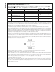
REFERENCE AND ANALOG INPUT CHARACTERISTICS
V
CM
Common Mode Input Voltage 1.0
0.5 V (min)
1.8 V (max)
C
IN
V
IN
Input Capacitance (each pin to
GND)
V
IN
= 2.5 Vdc
+ 0.7 V
rms
(CLK LOW) 8 pF
(CLK HIGH) 7 pF
V
REF
Reference Voltage (Note 13) 1.00
0.8 V (min)
1.5 V (max)
Reference Input Resistance 100 MΩ
ADC11DL066
www.national.com5