
Manual
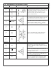
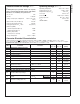

DC and Logic Electrical Characteristics
Unless otherwise specified, the following specifications apply for AGND = DGND = DR GND = 0V, V
A
=V
D
= +3.3V, V
DR
=
+2.5V, PD = 0V, INT/EXT REF pin = 3.3V, V
REF
= +1.0V, f
CLK
= 66 MHz, f
IN
= 10 MHz, t
r
=t
f
= 2 ns, C
L
= 15 pF/pin. Bold-
face limits apply for T
J
=T
MIN
to T
MAX
: all other limits T
J
= 25˚C (Notes 7, 8, 9)
Symbol Parameter Conditions
Typical
(Note 10)
Limits
(Note 10)
Units
(Limits)
CLK, PD, OE DIGITAL INPUT CHARACTERISTICS
V
IN(1)
Logical “1” Input Voltage V
D
= 3.6V 2.0 V (min)
V
IN(0)
Logical “0” Input Voltage V
D
= 3.0V 1.0 V (max)
I
IN(1)
Logical “1” Input Current V
IN
= 3.3V 10 µA
I
IN(0)
Logical “0” Input Current V
IN
= 0V −10 µA
C
IN
Digital Input Capacitance 5 pF
D0–D11 DIGITAL OUTPUT CHARACTERISTICS
V
OUT(1)
Logical “1” Output Voltage I
OUT
= −0.5 mA
V
DR
= 2.5V 2.3 V (min)
V
DR
=3V 2.7 V (min)
V
OUT(0)
Logical “0” Output Voltage I
OUT
= 1.6 mA, V
DR
=3V 0.4 V (max)
I
OZ
TRI-STATE
®
Output Current
V
OUT
= 2.5V or 3.3V 100 nA
V
OUT
= 0V −100 nA
+I
SC
Output Short Circuit Source
Current
V
OUT
= 0V −20 mA
−I
SC
Output Short Circuit Sink Current V
OUT
=V
DR
20 mA
C
OUT
Digital Output Capacitance 5 pF
POWER SUPPLY CHARACTERISTICS
I
A
Analog Supply Current
PD Pin = DGND, V
REF
= 1.0V
PD Pin = V
DR
197
14
237 mA (max)
mA
I
D
Digital Supply Current
PD Pin = DGND
PD Pin = V
DR
,f
CLK
=0
11
8.7
35 mA (max)
mA
I
DR
Digital Output Supply Current
PD Pin = DGND, C
L
= 0 pF (Note 14)
PD Pin = V
DR
,f
CLK
=0
<
2
0
mA
mA
Total Power Consumption
PD Pin = DGND, C
L
= 0 pF (Note 15)
PD Pin = V
DR
,f
CLK
=0
686
75
898 mW (max)
mW
PSRR1 Power Supply Rejection Ratio
Rejection of Full-Scale Error with
V
A
= 3.0V vs. 3.6V
56 dB
PSRR2 Power Supply Rejection Ratio
Rejection of Power Supply Noise with
10 MHz, 500 mV riding on V
A
44 dB
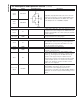
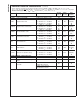
AC Electrical Characteristics
Unless otherwise specified, the following specifications apply for AGND = DGND = DR GND = 0V, V
A
=V
D
= +3.3V, V
DR
=
+2.5V, PD = 0V, INT/EXT REF pin = 3.3V, V
REF
= +1.0V, f
CLK
= 66 MHz, f
IN
= 10 MHz, t
r
=t
f
= 3 ns, C
L
= 15 pF/pin. Bold-
face limits apply for T
J
=T
MIN
to T
MAX
: all other limits T
J
= 25˚C (Notes 7, 8, 9, 12)
Symbol Parameter Conditions
Typical
(Note 10)
Limits
(Note 10)
Units
(Limits)
f
CLK
1
Maximum Clock Frequency 75 66 MHz (min)
f
CLK
2
Minimum Clock Frequency 15 MHz
t
CH
Clock High Time 6.6 ns (min)
t
CL
Clock Low Time 6.6 ns (min)
t
CONV
Conversion Latency 6
Clock
Cycles
t
OD
Data Output Delay after Rising
CLK Edge
V
DR
= 2.5V
rising 6.6 9.0 ns (max)
falling 5.0 8.5 ns (max)
V
DR
= 3.3V
rising 5.4 9.0 ns (max)
falling 5.6 9.0 ns (max)
t
AD
Aperture Delay 2 ns
ADC11DL066
www.national.com7