
Manual
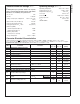

AC Electrical Characteristics (Continued)
Unless otherwise specified, the following specifications apply for AGND = DGND = DR GND = 0V, V
A
=V
D
= +3.3V, V
DR
=
+2.5V, PD = 0V, INT/EXT REF pin = 3.3V, V
REF
= +1.0V, f
CLK
= 66 MHz, f
IN
= 10 MHz, t
r
=t
f
= 3 ns, C
L
= 15 pF/pin. Bold-
face limits apply for T
J
=T
MIN
to T
MAX
: all other limits T
J
= 25˚C (Notes 7, 8, 9, 12)
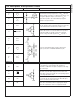
Symbol Parameter Conditions
Typical
(Note 10)
Limits
(Note 10)
Units
(Limits)
t
AJ
Aperture Jitter 1.2 ps rms
t
HOLD
Clock Edge to Data Transition 8 ns
t
DIS
Data outputs into TRI-STATE
Mode
10 ns
t
EN
Data Outputs Active after
TRI-STATE
10 ns
t
PD
Power Down Mode Exit Cycle
0.1 µF on pins 4, 14; series 1.5 Ω &1
µF between pins 5, 6 and between
pins 12, 13
500 µs
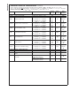
Note 1: Absolute Maximum Ratings indicate limits beyond which damage to the device may occur. Operating Ratings indicate conditions for which the device is
functional, but do not guarantee specific performance limits. For guaranteed specifications and test conditions, see the Electrical Characteristics. The guaranteed
specifications apply only for the test conditions listed. Some performance characteristics may degrade when the device is not operated under the listed test
conditions.
Note 2: All voltages are measured with respect to GND = AGND = DGND = 0V, unless otherwise specified.
Note 3: When the input voltage at any pin exceeds the power supplies (that is, V
IN
<
AGND, or V
IN
>
V
A
), the current at that pin should be limited to 25 mA. The
50 mA maximum package input current rating limits the number of pins that can safely exceed the power supplies with an input current of 25 mA to two.
Note 4: The absolute maximum junction temperature (T
J
max) for this device is 150˚C. The maximum allowable power dissipation is dictated by T
J
max, the
junction-to-ambient thermal resistance (θ
JA
), and the ambient temperature, (T
A
), and can be calculated using the formula P
D
MAX=(T
J
max - T
A
)/θ
JA
. In the 64-pin
TQFP, θ
JA
is 50˚C/W, so P
D
MAX=2Watts at 25˚C and 800 mW at the maximum operating ambient temperature of 85˚C. Note that the power consumption of this
device under normal operation will typically be about 726 mW (686 typical power consumption + 40 mW TTL output loading). The values for maximum power
dissipation listed above will be reached only when the device is operated in a severe fault condition (e.g. when input or output pins are driven beyond the power
supply voltages, or the power supply polarity is reversed). Obviously, such conditions should always be avoided.
Note 5: Human body model is 100 pF capacitor discharged through a 1.5 kΩ resistor. Machine model is 220 pF discharged through 0Ω.
Note 6: The 235˚C reflow temperature refers to infrared reflow. For Vapor Phase Reflow (VPR), the following Conditions apply: Maintain the temperature at the top
of the package body above 183˚C for a minimum 60 seconds. The temperature measured on the package body must not exceed 220˚C. Only one excursion above
183˚C is allowed per reflow cycle.
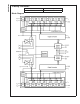
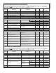
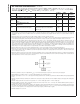
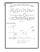
Note 7: The inputs are protected as shown below. Input voltage magnitudes above V
A
or below GND will not damage this device, provided current is limited per
(Note 3). However, errors in the A/D conversion can occur if the input goes above V
A
or below GND by more than 100 mV. As an example, if V
A
is +3.3V, the full-scale
input voltage must be ≤+3.4V to ensure accurate conversions.
20077307
Note 8: To guarantee accuracy, it is required that |V
A
–V
D
| ≤ 100 mV and separate bypass capacitors are used at each power supply pin.
Note 9: With the test condition for V
REF
= +1.0V (2V
P-P
differential input), the 11-bit LSB is 976 µV.
Note 10: Typical figures are at T
J
= 25˚C, and represent most likely parametric norms. Test limits are guaranteed to National’s AOQL (Average Outgoing Quality
Level).
Note 11: Integral Non Linearity is defined as the deviation of the analog value, expressed in LSBs, from the straight line that passes through positive and negative
full-scale.
Note 12: Timing specifications are tested at TTL logic levels, V
IL
= 0.4V for a falling edge and V
IH
= 2.4V for a rising edge.
Note 13: Optimum performance will be obtained by keeping the reference input in the 0.8V to 1.5V range. The LM4051CIM3-ADJ (SOT-23 package) is
recommended for external reference applications.
Note 14: I
DR
is the current consumed by the switching of the output drivers and is primarily determined by load capacitance on the output pins, the supply voltage,
V
DR
, and the rate at which the outputs are switching (which is signal dependent). I
DR
=V
DR
(C
0
xf
0
+C
1
xf
1
+....C
10
xf
10
) where V
DR
is the output driver power supply
voltage, C
n
is total capacitance on the output pin, and f
n
is the average frequency at which that pin is toggling.
Note 15: Excludes I
DR
. See note 14.
ADC11DL066
www.national.com 8