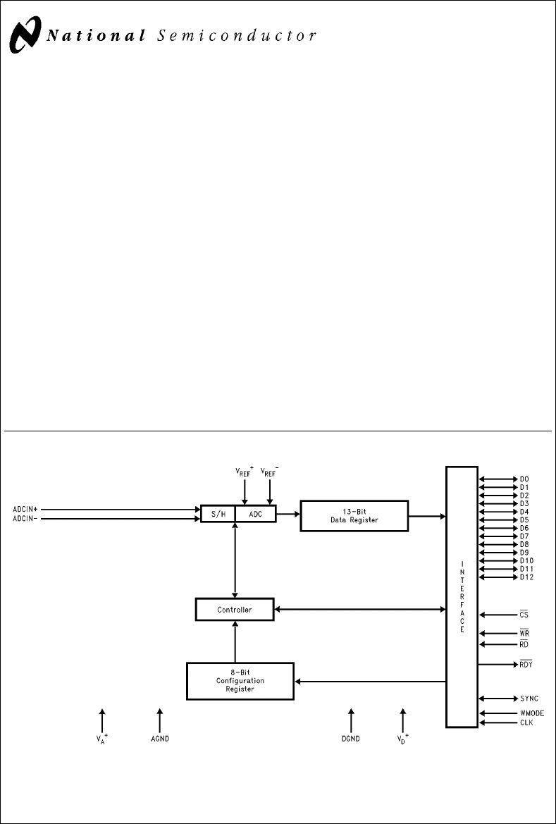
ADC12041 12-Bit Plus Sign 216 kHz Sampling Analog-to-Digital Converter Y General Description Y Operating from a single 5V power supply the ADC12041 is a 12 bit a sign, parallel I/O, self-calibrating, sampling analogto-digital converter (ADC). The maximum sampling rate is 216 kHz. On request, the ADC goes through a self-calibration process that adjusts linearity, zero and full-scale errors.
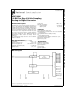
Connection Diagrams 28-Pin PLCC 28-Pin SSOP TL/H/12441 – 3 Order Number ADC12041CIV See NS Package Number V28A TL/H/12441–2 Order Number ADC12041CIMSA See NS Package Number MSA28 Ordering Information Industrial Temperature Range b 40§ C s TA s a 85§ C NS Package Number ADC12041CIV V28A ADC12041CIMSA MSA28, SSOP 2
Absolute Maximum Ratings Operating Ratings (Notes 1 and 2) (Notes 1 and 2) Temperature Range (Tmin s TA s Tmax) Supply Voltage (VA a and VD a ) Voltage at all Inputs lVA a b VD a l lAGND b DGNDl Input Current at Any Pin (Note 3) Package Input Current (Note 3) Power Dissipation (Note 4) at TA e 25§ C Storage Temperature Lead Temperature SSOP Package Vapor Phase (60 sec.) Infared (15 sec.) V Package, Infared (15 sec.) 6.0V b 0.3V to V a a 0.3V 4.5V to 5.
Power Supply Characteristics The following specifications apply to the ADC12041 for VA a e VD a e 5V, VREF a e 4.096V, VREFb e 0.0V, 12-bit a sign conversion mode, fCLK e 12.0 MHz, RS e 25X, source impedance for VREF a and VREFb 1X, fully differential input with fixed 2.048V common-mode voltage, and minimum acquisition time, unless otherwise specified.
Digital Logic Input/Output Characteristics The following specifications apply to the ADC12041 for VA a e VD a e 5V, VREF a e 4.096V, VREFb e 0.0V, 12-bit a sign conversion mode, fCLK e 12.0 MHz, RS e 25X, source impedance for VREF a and VREFb s 1X, fully differential input with fixed 2.048V common-mode voltage, and minimum acquisition time, unless otherwise specified.
Digital Timing Characteristics The following specifications apply to the ADC12041, 13-bit data bus width, VA a e VD a e 5V, fCLK e 12 MHz, tf e 3 ns and CL e 50 pF on data I/O lines Symbol (Figure 7) Parameter tTPR Throughput Rate tCSWR Conditions Limits (Note 11) Unit (Limit) 222 kHz Falling Edge of CS to Falling Edge of WR 0 ns tWRCS Active Edge of WR to Rising Edge of CS 0 ns tWR WR Pulse Width 30 ns (min) tWRSETFalling Write Setup Time WMODE e ‘‘1’’ 20 ns (min) tWRHOLDFalling
Notes on Specifications (Continued) Note 6: Each input is protected by a nominal 6.5V breakdown voltage zener diode to GND, as shown below, input voltage magnitude up to 5V above VA a or 5V below GND will not damage the ADC12041. There are parasitic diodes that exist between the inputs and the power supply rails and errors in the A/D conversion can occur if these diodes are forward biased by more than 50 mV. As an example, if VA a is 4.50 VDC, full-scale input voltage must be 4.
Electrical Characteristics TL/H/12441 – 5 FIGURE 1. Output Digital Code vs the Operating Input Voltage Range (General Case) TL/H/12441 – 6 FIGURE 2. Output Digital Code vs the Operating Input Voltage Range for VREF e 4.
Electrical Characteristics (Continued) TL/H/12441 – 7 FIGURE 3. VREF Operating Range (General Case) TL/H/12441 – 8 FIGURE 4.
Electrical Characteristics (Continued) TL/H/12441 – 9 FIGURE 5a. Transfer Characteristic TL/H/12441 – 10 FIGURE 5b.
Electrical Characteristics (Continued) TL/H/12441 – 11 FIGURE 5c. Simplified Error vs Output Code after Auto-Calibration Cycle TL/H/12441 – 12 FIGURE 6.
Timing Diagrams TL/H/12441 – 13 FIGURE 7a. Sync-Out Write (WMODE e 1, BW e 1), Read and Convert Cycles TL/H/12441 – 14 FIGURE 7b.
Timing Diagrams (Continued) TL/H/12441 – 46 FIGURE 7c. Sync-Out Write (WMODE e 0, BW e 1), Read and Convert Cycles TL/H/12441 – 47 FIGURE 7d.
Timing Diagrams (Continued) TL/H/12441 – 48 FIGURE 7e. Sync-Out Read and Convert Cycles TL/H/12441 – 49 FIGURE 7f.
Timing Diagrams (Continued) TL/H/12441 – 50 FIGURE 7g. 8-bit Bus Read Cycle (Sync-Out) TL/H/12441 – 51 FIGURE 7h.
Timing Diagrams (Continued) TL/H/12441 – 15 FIGURE 7i. Write Signal Negates RDY (Writing the Standby, Auto-Cal or Auto-Zero Command) TL/H/12441 – 16 FIGURE 7j.
Typical Performance Characteristics (See Note 19, Electrical Characteristic Section) Integral Linearity Error (INL) Change vs Clock Frequency Full-Scale Error Change vs Clock Frequency TL/H/12441 – 18 TL/H/12441–17 Integral Linearity Error (INL) Change vs Temperature Full-Scale Error Change vs Temperature TL/H/12441 – 21 TL/H/12441–20 Integral Linearity Error (INL) Change vs Reference Voltage Full-Scale Error Change vs Reference Voltage TL/H/12441 – 24 TL/H/12441–23 Integral Linearity Error (INL
Typical Performance Characteristics (See Note 21, Electrical Characteristic Section) (Continued) Reference Current vs Clock Frequency Supply Current vs Clock Frequency TL/H/12441–29 TL/H/12441 – 30 Analog Supply Current vs Temperature Digital Supply Current vs Temperature TL/H/12441–31 TL/H/12441 – 32 18
Typical Performance Characteristics (Continued) The curves were obtained under the following conditions. RS e 50X, TA e 25§ C, VA a e VD a e 5V, VREF e 4.096V, fCLK e 12 MHz, and the sampling rate fS e 215 kHz unless otherwise stated.
Pin Description PLCC and SSOP Pkg. Pin Number Pin Name Description 5 6 VIN a VINb The analog ADC inputs. VIN a is the non-inverting (positive) input and VINb is the inverting (negative) input into the ADC. 10 VREF a Positive reference input. The operating voltage range for this input is 1V s VREF a s VA a (see Figures 3 and 4 ). This pin should be bypassed to AGND at least with a parallel combination of a 10 mF and a 0.1 mF (ceramic) capacitor.
Register Bit Description CONFIGURATION REGISTER (Write Only) This is an 8-bit write-only register that is used to program the functionality of the ADC12041. All data written to the ADC12041 will always go to this register only. The contents of this register cannot be read. MSB LSB b7 b6 b5 COMMAND FIELD b4 b3 b2 b1 b0 SYNC BW SE ACQ TIME Power on State: 10 Hex b1 – b0: The ACQ TIME bits select one of four possible acquistion times in the SYNC-OUT mode (b4 e 0).
SYNC/ASYNC MODE Functional Description The ADC12041 may be programmed to operate in synchronous (SYNC-IN) or asynchronous (SYNC-OUT) mode. To enter synchronous mode, the SYNC bit in the Configuration register must be set. The ADC12041 is in synchronous mode after a hardware power-up. In this mode, the SYNC pin is programmed as an input and conversions are synchronized to the rising edges of the signal applied at the SYNC pin.
Features and Operating Modes (Continued) 13-bit mode: A Ful-Cal or Auto-Zero command must be issued and the BW bit (b3) set. The active edge of the write pulse on the WR pin will force the RDY signal high. At this time the converter begins executing a full calibration or auto-zero cycle. The RDY signal will automatically go low when the full calibration or auto-zero cycle is done.
Features and Operating Modes (Continued) SYNC-IN/Synchronous For the SYNC-IN case, it is assumed that a series of SYNC pulses at the desired sampling rate are applied at the SYNC pin of the ADC12041. 8-bit mode: A write to the ADC12041 should set the SYNC bit, write the START command and clear the BW bit. The programmed acquisition time in bits b1 and b0 is a don’t care condition in the SYNC-IN mode.
Analog Application Information REFERENCE VOLTAGE The ADC12041 has two reference inputs, VREF a and VREFb. They define the zero to full-scale range of the analog input signals over which 4095 positive and 4096 negative codes exist. The reference inputs can be connected to span the entire supply voltage range (VREFb e AGND, VREF a e VA a ) or they can be connected to different voltages when other input spans are required. The reference inputs of the ADC12041 have transient capacitive switching currents.
Analog Application Information (Continued) on the PC board. All supply currents should be supplied by the capacitor instead of being drawn from the external supply lines, while the external supply charges the capacitor at a steady rate. The ADC has two VD a and DGND pins. It is recommended to use a 0.1 mF plus a 10 mF capacitor between pin 21(VD a ) and 22 (DGND) the SSOP and PLCC package. The layout diagram in Figure 10 shows the recommended placement for the supply bypass capacitors.
Analog Application Information (Continued) TL/H/12441 – 45 FIGURE 10. Top View of Printed Circuit Board for a 28-Pin PLCC ADC12041 between the VREF a and VREFb, and by bypassing in a manner similar to that described for the supply pins. When a single ended reference is used, VREFb is connected to AGND and only two capacitors are used between VREF a and VREFb (0.1 mF a 10 mF).
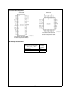
Physical Dimensions inches (millimeters) 28-Lead Molded Plastic Leaded Chip Carrier Order Number ADC12041CIV NS Package Number V28A 29
ADC12041 12-Bit Plus Sign 216 kHz Sampling Analog-to-Digital Converter Physical Dimensions inches (millimeters) (Continued) 28-Lead SSOP Order Number ADC12041CIMSA NS Package Number MSA28 LIFE SUPPORT POLICY NATIONAL’S PRODUCTS ARE NOT AUTHORIZED FOR USE AS CRITICAL COMPONENTS IN LIFE SUPPORT DEVICES OR SYSTEMS WITHOUT THE EXPRESS WRITTEN APPROVAL OF THE PRESIDENT OF NATIONAL SEMICONDUCTOR CORPORATION. As used herein: 1.