ADC12L080 12-Bit, 80 MSPS, 450 MHz Bandwidth A/D Converter with Internal Reference General Description Features The ADC12L080 is a monolithic CMOS analog-to-digital converter capable of converting analog input signals into 12-bit digital words at 80 Megasamples per second (MSPS). This converter uses a differential, pipeline architecture with digital error correction and an on-chip sample-and-hold circuit to minimize die size and power consumption while providing excellent dynamic performance.
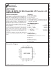
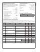
ADC12L080 Ordering Information Industrial (−40˚C ≤ TA ≤ +85˚C) Package ADC12L080CIVY 32 Pin LQFP ADC12L080EVAL Evaluation Board Block Diagram 20061002 www.national.
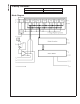
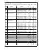
ADC12L080 Pin Descriptions and Equivalent Circuits Pin No. Symbol Equivalent Circuit Description ANALOG I/O 2 VIN+ 3 VIN− 1 VREF 31 VRP 32 VRM 30 VRN Differential analog signal Input pins. With a 1.0V reference voltage the full-scale differential input signal level is 2.0 VP-P with each input pin centered on a common mode voltage, VCM. The VIN- pin may be connected to VCM for single-ended operation, but a differential input signal is required for best performance. Reference input.
ADC12L080 Pin Descriptions and Equivalent Circuits Pin No. Symbol 14–19, 22–27 D0–D11 Equivalent Circuit (Continued) Description Digital data output pins that make up the 12-bit conversion results. D0 is the LSB, while D11 is the MSB of the output word. ANALOG POWER 5, 6, 29 VA 4, 7, 28 AGND Positive analog supply pins. These pins should be connected to a quiet +3.3V source and bypassed to AGND with 0.1 µF low ESL capacitors located within 1 cm of these power pins, and with a 10 µF capacitor.
Operating Ratings (Notes 1, 2) (Notes 1, 2) Operating Temperature If Military/Aerospace specified devices are required, please contact the National Semiconductor Sales Office/ Distributors for availability and specifications. Supply Voltage (VA, VD) VA, VD, VDR ≤ 100 mV VDR–VD ≤ 300 mV Voltage on Any Pin +2.4V to VD VREF 0.8V to 1.5V CLK, PD, OF −0.05V to VD + 0.05V VIN Input −0V to (VA − 0.5V) VCM −0.3V to VA or (VD + 0.3V) 0.5V to (VA-1.
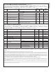
ADC12L080 DC and Logic Electrical Characteristics Unless otherwise specified, the following specifications apply for AGND = DGND = DR GND = 0V, VA = VD = +3.3V, VDR = +2.5V, PD = 0V, VREF = +1.0V external, VCM = 1.65V, RS < 100Ω, fCLK = 80 MHz, tr = tf = 2 ns, fIN = 70 MHz, CL = 15 pF/pin.
(Continued) Unless otherwise specified, the following specifications apply for AGND = DGND = DR GND = 0V, VA = VD = +3.3V, VDR = +2.5V, PD = 0V, VREF = +1.0V external, VCM = 1.65V, RS < 100Ω, fCLK = 80 MHz, tr = tf = 2 ns, fIN = 70 MHz, CL = 15 pF/pin.
ADC12L080 AC Electrical Characteristics (Continued) 20061007 Note 8: To guarantee accuracy, it is required that |VA–VD| ≤ 100 mV and separate bypass capacitors are used at each power supply pin. Note 9: With the test condition for VREF = +1.0V (2 VP-P differential input), the 12-bit LSB is 488 µV. Note 10: Typical figures are at TA = TJ = 25˚C, and represent most likely parametric norms. Test limits are guaranteed to National’s AOQL (Average Outgoing Quality Level).
APERTURE DELAY is the time after the rising edge of the clock to when the input signal is acquired or held for conversion. APERTURE JITTER (APERTURE UNCERTAINTY) is the variation in aperture delay from sample to sample. Aperture jitter manifests itself as noise in the output. COMMON MODE VOLTAGE (VCM) is the d.c. potential present at both signal inputs to the ADC. POWER SUPPLY REJECTION RATIO (PSRR) is a measure of how well the ADC rejects a change in the power supply voltage.
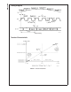
ADC12L080 Timing Diagram 20061009 Output Timing Transfer Characteristic 20061010 FIGURE 1. Transfer Characteristic www.national.
ADC12L080 Typical Performance Characteristics DNL, INL VA = VD = 3.3V, VDR = 2.5V, VREF = 1.0V external, VCM = 1.65V, fCLK = 80 MHz, fIN = 0, unless otherwise stated. DNL INL 20061041 20061045 DNL vs. fCLK INL vs. fCLK 20061042 20061046 DNL vs. Clock Duty Cycle INL vs. Clock Duty Cycle 20061043 20061047 11 www.national.
ADC12L080 Typical Performance Characteristics DNL, INL VA = VD = 3.3V, VDR = 2.5V, VREF = 1.0V external, VCM = 1.65V, fCLK = 80 MHz, fIN = 0, unless otherwise stated. (Continued) DNL vs. Temperature INL vs. Temperature 20061044 20061048 DNL vs. VDR INL vs. VDR 20061070 www.national.
ADC12L080 Typical Performance Characteristics VA = VD = 3.3V, VDR = 2.5V, VREF = 1.0V external, VCM = 1.65V, fCLK = 80 MHz, fIN = 70 MHz, unless otherwise stated. Distortion vs. VA SNR,SINAD,SFDR vs. VA 20061049 20061056 SNR,SINAD,SFDR vs. VDR Distortion vs. VDR 20061050 20061057 SNR,SINAD,SFDR vs. VCM Distortion vs. VCM 20061051 20061058 13 www.national.
ADC12L080 Typical Performance Characteristics VA = VD = 3.3V, VDR = 2.5V, VREF = 1.0V external, VCM = 1.65V, fCLK = 80 MHz, fIN = 70 MHz, unless otherwise stated. (Continued) SNR,SINAD,SFDR vs. fCLK Distortion vs. fCLK 20061052 20061059 SNR,SINAD,SFDR vs. Clock Duty Cycle Distortion vs. Clock Duty Cycle 20061053 20061060 SNR,SINAD,SFDR vs. VREF Distortion vs. VREF 20061054 www.national.
ADC12L080 Typical Performance Characteristics VA = VD = 3.3V, VDR = 2.5V, VREF = 1.0V external, VCM = 1.65V, fCLK = 80 MHz, fIN = 70 MHz, unless otherwise stated. (Continued) SNR,SINAD,SFDR vs. fIN Distortion vs. fIN 20061072 20061073 SNR,SINAD,SFDR vs. Temperature Distortion vs. Temperature 20061055 20061062 Spectral Response @ 10 MHz Input tOD vs. VDR 20061063 20061064 15 www.national.
ADC12L080 Typical Performance Characteristics VA = VD = 3.3V, VDR = 2.5V, VREF = 1.0V external, VCM = 1.65V, fCLK = 80 MHz, fIN = 70 MHz, unless otherwise stated. (Continued) Spectral Response @ 40 MHz Input Spectral Response @ 70 MHz Input 20061065 20061066 Intermodulation Distortion, fIN1= 19.6 MHz, fIN2 = 20.5 MHz Spectral Response @ 150 MHz Input 20061068 www.national.
Operating on a single +3.3V supply, the ADC12L080 uses a pipeline architecture with error correction circuitry to help ensure maximum performance. Differential analog input signals are digitized to 12 bits. Each analog input signal should have a peak-to-peak voltage equal to the input reference voltage, VREF, be centered around VREF and be 180˚ out of phase with each other. Table 1 and Table 2 indicate the input to output relationship of the ADC12L080.
ADC12L080 Applications Information TABLE 3. Resistor values for Circuit of Figure 5 (Continued) The full scale error in LSB for a sine wave input can be described as approximately SIGNAL RANGE EFS = 4096 ( 1 - sin (90˚ + dev)) 0 - 0.25V 0Ω open 200Ω 1780Ω 1000Ω Where dev is the angular difference between the two signals having a 180˚ relative phase relationship to each other (see Figure 3). Drive the analog inputs with a source impedance less than 100Ω. 0 - 0.
conversion, the more instantaneous digital current flows through VDR and DR GND. These large charging current spikes can cause on-chip noise and couple into the analog circuitry, degrading dynamic performance. Adequate bypassing, limiting output capacitance and careful attention to the ground plane will reduce this problem. Additionally, bus capacitance beyond the specified 15 pF/pin will cause tOD to increase, making it difficult to properly latch the ADC output data.
ADC12L080 Applications Information (Continued) 20061014 FIGURE 5. Differential Drive Circuit of Figure 4 20061015 FIGURE 6. Driving the Signal Inputs with a Transformer www.national.
nificant impact upon system noise performance. The best logic family to use in systems with A/D converters is one which employs non-saturating transistor designs, or has low noise characteristics, such as the 74LS, 74HC(T) and 74AC(T)Q families. The worst noise generators are logic families that draw the largest supply current transients during clock or signal edges, like the 74F and the 74AC(T) families. (Continued) 5.
ADC12L080 Applications Information cause faulty or erratic operation. It is not uncommon for high speed digital components (e.g., 74F and 74AC devices) to exhibit overshoot or undershoot that goes above the power supply or below ground. A resistor of about 50Ω to 100Ω in series with any offending digital input, close to the signal source, will eliminate the problem. Do not allow input voltages to exceed the supply voltage, even on a transient basis. Not even during power up or power down.
inches (millimeters) unless otherwise noted 32-Lead LQFP Package Ordering Number ADC12L080CIVY NS Package Number VBE32A National does not assume any responsibility for use of any circuitry described, no circuit patent licenses are implied and National reserves the right at any time without notice to change said circuitry and specifications. For the most current product information visit us at www.national.com.