
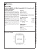
Instruction Manual
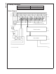
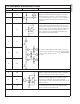
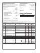
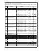
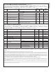

Pin Descriptions and Equivalent Circuits
Pin No. Symbol Equivalent Circuit Description
ANALOG I/O
2V
IN
+
Differential analog signal Input pins. With a 1.0V reference
voltage the full-scale differential input signal level is 2.0 V
P-P
with each input pin centered on a common mode voltage,
V
CM
. The V
IN
- pin may be connected to V
CM
for single-ended
operation, but a differential input signal is required for best
performance.
3V
IN
−
1V
REF
Reference input. This pin should be connected to V
A
to use
the internal 1.0V reference. If it is desired to use an external
reference voltage, this pin should be bypassed to AGND with
a 0.1 µF low ESL capacitor. Specified operation is with a
V
REF
of 1.0V, but the device will function well with a V
REF
range indicated in the Electrical Tables.
31 V
RP
These pins are high impedance reference bypass pins only.
Connect a 0.1 µF capacitor from each of these pins to AGND.
Connect a 1.0 µF capacitor from V
RP
to V
RN
. DO NOT LOAD
these pins.
32 V
RM
30 V
RN
DIGITAL I/O
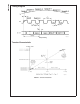
10 CLK
Digital clock input. The range of frequencies for this input is
10 MHz to 80 MHz with guaranteed performance at 80 MHz.
The input is sampled on the rising edge of this input.
11 OF
Output format selection. When this pin is LOW, the output
format is offset binary. When this pin is HIGH the output
format is two’s complement. This pin may be changed
asynchronously, but such a change will result in errors for one
or two conversions.
8PD
PD is the Power Down input pin. When high, this input puts
the converter into the power down mode. When this pin is
low, the converter is in the active mode.
ADC12L080
www.national.com3