
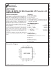
Instruction Manual
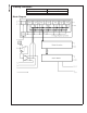
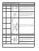
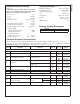

Pin Descriptions and Equivalent Circuits (Continued)
Pin No. Symbol Equivalent Circuit Description
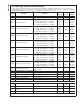
14–19,
22–27
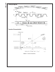
D0–D11
Digital data output pins that make up the 12-bit conversion
results. D0 is the LSB, while D11 is the MSB of the output
word.
ANALOG POWER
5, 6, 29 V
A
Positive analog supply pins. These pins should be connected
to a quiet +3.3V source and bypassed to AGND with 0.1 µF
low ESL capacitors located within 1 cm of these power pins,
and with a 10 µF capacitor.
4, 7, 28 AGND The ground return for the analog supply.
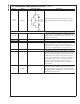
DIGITAL POWER
13 V
D
Positive digital supply pin. This pin should be connected to
the same quiet +3.3V source as is V
A
and bypassed to
DGND with a 0.1 µF monolithic capacitor in parallel with a 10
µF capacitor, both located within 1 cm of the power pin.
9, 12 DGND The ground return for the digital supply.
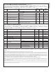
21 V
DR
Positive digital supply pin for the ADC12L080’s output drivers.
This pin should be connected to a voltage source in the range
indicated in the Operating Ratings table and be bypassed to
DR GND with a 0.1 µF capacitor. If the supply for this pin is
different from the supply used for V
A
and V
D
, it should also be
bypassed with a 10 µF capacitor. The voltage at this pin
should never exceed the voltage on V
D
by more than
300 mV. All bypass capacitors should be located within 1 cm
of the supply pin.
20 DR GND
The ground return for the digital supply for the ADC12L080’s
output drivers. This pin should be connected to the system
digital ground, but not be connected in close proximity to the
ADC12L080’s DGND or AGND pins. See Section 6.0 (Layout
and Grounding) for more details.
ADC12L080
www.national.com 4