
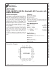
Instruction Manual
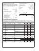

DC and Logic Electrical Characteristics
Unless otherwise specified, the following specifications apply for AGND = DGND = DR GND = 0V, V
A
=V
D
= +3.3V, V
DR
=
+2.5V, PD = 0V, V
REF
= +1.0V external, V
CM
= 1.65V, R
S
<
100Ω,f
CLK
= 80 MHz, t
r
=t
f
= 2 ns, f
IN
= 70 MHz, C
L
= 15 pF/pin.
Boldface limits apply for T
J
=T
MIN
to T
MAX
: all other limits T
J
= 25˚C (Notes 7, 8, 9, 10)
Symbol Parameter Conditions
Typical
(Note 10)
Limits
(Note 10)
Units
(Limits)
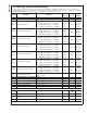
DYNAMIC CONVERTER CHARACTERISTICS
BW Full Power Bandwidth -0.5 dBFS Input, Output at −3 dB 450 MHz
SNR Signal-to-Noise Ratio
f
IN
= 10 MHz, Differential V
IN
= −0.5 dBFS 66 64 dB (min)
f
IN
= 40 MHz, Differential V
IN
= −0.5 dBFS 65 dB
f
IN
= 70 MHz, Differential V
IN
= −0.5 dBFS 65 63 dB (min)
f
IN
= 150 MHz, Differential V
IN
= −0.5 dBFS 63 dB
SINAD Signal-to-Noise & Distortion
f
IN
= 10 MHz, Differential V
IN
= −0.5 dBFS 66 63 dB (min)
f
IN
= 40 MHz, Differential V
IN
= −0.5 dBFS 64.5 dB
f
IN
= 70 MHz, Differential V
IN
= −0.5 dBFS 64 62.7 dB (min)
f
IN
= 150 MHz, Differential V
IN
= −0.5 dBFS 62 dB
ENOB Effective Number of Bits
f
IN
= 10 MHz, Differential V
IN
= −0.5 dBFS 10.7 10.2 Bits (min)
f
IN
= 40 MHz, Differential V
IN
= 0.5 dBFS 10.4 Bits
f
IN
= 70 MHz, Differential V
IN
= −0.5 dBFS 10.3 10.1 Bits (min)
f
IN
= 150 MHz, Differential V
IN
= −0.5 dBFS 10.0 Bits
THD Total Harmonic Distortion
f
IN
= 10 MHz, Differential V
IN
= −0.5 dBFS −77 -66 dB (max)
f
IN
= 40 MHz, Differential V
IN
= −0.5 dBFS -74 dB
f
IN
= 70 MHz, Differential V
IN
= −0.5 dBFS -71 -65 dB (max)
f
IN
= 150 MHz, Differential V
IN
= −0.5 dBFS -70 dB
2nd
Harm
Second Harmonic Distortion
f
IN
= 10 MHz, Differential V
IN
= −0.5 dBFS −80 -68 dB (max)
f
IN
= 40 MHz, Differential V
IN
= −0.5 dBFS -80 dB
f
IN
= 70 MHz, Differential V
IN
= −0.5 dBFS -80 -65.5 dB (max)
f
IN
= 150 MHz, Differential V
IN
= −0.5 dBFS -79 dB
3rd
Harm
Third Harmonic Distortion
f
IN
= 10 MHz, Differential V
IN
= −0.5 dBFS −84 -69 dB (max)
f
IN
= 40 MHz, Differential V
IN
= −0.5 dBFS -81 dB
f
IN
= 70 MHz, Differential V
IN
= −0.5 dBFS -79 -66 dB (max)
f
IN
= 150 MHz, Differential V
IN
= −0.5 dBFS -78 dB
SFDR Spurious Free Dynamic Range
f
IN
= 10 MHz, Differential V
IN
= −0.5 dBFS 80 68 dB (min)
f
IN
= 40 MHz, Differential V
IN
= −0.5 dBFS 77 dB
f
IN
= 70 MHz, Differential V
IN
= −0.5 dBFS 74 -65.5 dB (min)
f
IN
= 150 MHz, Differential V
IN
= −0.5 dBFS 73 dB
IMD Intermodulation Distortion
f
IN
1 = 19.6MHz, f
IN
2 = 20.5 MHz,
each = -6.0 dBFS
66 dBFS
CLK, PD, OF DIGITAL INPUT CHARACTERISTICS
V
IN(1)
Logical “1” Input Voltage V
D
= 3.3V 2.0 V (min)
V
IN(0)
Logical “0” Input Voltage V
D
= 3.3V 0.8 V (max)
I
IN(1)
Logical “1” Input Current V
IN
+, V
IN
− = 3.3V 10 µA
I
IN(0)
Logical “0” Input Current V
IN
+, V
IN
− = 0V −10 µA
C
IN
Digital Input Capacitance 5 pF
D0–D11 DIGITAL OUTPUT CHARACTERISTICS
V
OUT(1)
Logical “1” Output Voltage I
OUT
= −0.5 mA
V
DR
−
0.18
V (min)
V
OUT(0)
Logical “0” Output Voltage I
OUT
= 1.6 mA 0.4 V (max)
+I
SC
Output Short Circuit Source
Current
V
OUT
= 0V −20 mA
−I
SC
Output Short Circuit Sink Current V
OUT
= 2.5V 20 mA
ADC12L080
www.national.com 6