
Instruction Manual

DC and Logic Electrical Characteristics (Continued)
Unless otherwise specified, the following specifications apply for AGND = DGND = DR GND = 0V, V
A
=V
D
= +3.3V, V
DR
=
+2.5V, PD = 0V, V
REF
= +1.0V external, V
CM
= 1.65V, R
S
<
100Ω,f
CLK
= 80 MHz, t
r
=t
f
= 2 ns, f
IN
= 70 MHz, C
L
= 15 pF/pin.
Boldface limits apply for T
J
=T
MIN
to T
MAX
: all other limits T
J
= 25˚C (Notes 7, 8, 9, 10)
Symbol Parameter Conditions
Typical
(Note 10)
Limits
(Note 10)
Units
(Limits)
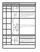
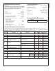
POWER SUPPLY CHARACTERISTICS
I
A
Analog Supply Current
PD Pin = DGND
PD Pin = V
DR
120
10
168 mA (max)
mA
I
D
Digital Supply Current
PD Pin = DGND
PD Pin = V
DR
6
5
11.5 mA (max)
mA
I
DR
Digital Output Supply Current
PD Pin = DGND, f
in
= 0, (Note 13)
PD Pin = V
DR
<
1
0
mA
mA
Total Power Consumption
PD Pin = DGND, C
L
= 0 pF (Note 14)
PD Pin = V
DR
425
50
590 mW (max)
mW
PSRR1 Power Supply Rejection Ratio
Rejection of Full-Scale Gain Error
change with V
A
= 3.0V vs. 3.6V
41 dB
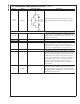
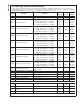
AC Electrical Characteristics
Unless otherwise specified, the following specifications apply for AGND = DGND = DR GND = 0V, V
A
=V
D
= +3.3V, V
DR
=
+2.5V, PD = 0V, V
REF
= +1.0V external, V
CM
= 1.65V, R
S
<
100Ω,f
CLK
= 80 MHz, t
r
=t
f
= 2 ns, f
IN
= 70 MHz, C
L
= 15 pF/pin.
Boldface limits apply for T
J
=T
MIN
to T
MAX
: all other limits T
J
= 25˚C (Notes 7, 8, 9, 10, 11)
Symbol Parameter Conditions
Typical
(Note 10)
Limits
(Note 10)
Units
(Limits)
Maximum Clock Frequency 80 MHz (min)
Minimum Clock Frequency 10 MHz
Clock Duty Cycle
60
40
% (max)
% (min)
t
CH
Clock High Time 5.5 ns (min)
t
CL
Clock Low Time 5.5 ns (min)
t
CONV
Conversion Latency 6
Clock
Cycles
t
OD
Data Output Delay after Rising
CLK Edge
V
DR
= 2.5V 5.2 8.3 ns (max)
V
DR
= 3.3V 4.8 7.5 ns (max)
t
AD
Aperture Delay 2 ns
t
AJ
Aperture Jitter 0.7 ps rms
t
PD
Power Down Mode Exit Cycle
0.1 µF on pins 30, 31, 32,
and 1.0 µF from pin 30 to 31
1µs
Note 1: Absolute Maximum Ratings indicate limits beyond which damage to the device may occur. Operating Ratings indicate conditions for which the device is
functional, but do not guarantee specific performance limits. For guaranteed specifications and test conditions, see the Electrical Characteristics. The guaranteed
specifications apply only for the test conditions listed. Some performance characteristics may degrade when the device is not operated under the listed test
conditions.
Note 2: All voltages are measured with respect to GND = AGND = DGND = 0V, unless otherwise specified.
Note 3: When the input voltage at any pin exceeds the power supplies (that is, V
IN
<
AGND, or V
IN
>
V
A
,V
D
or V
DR
), the current at that pin should be limited to
25 mA. The 50 mA maximum package input current rating limits the number of pins that can safely exceed the power supplies with an input current of 25 mA to two.
Note 4: The absolute maximum junction temperature (T
J
max) for this device is 150˚C. The maximum allowable power dissipation is dictated by T
J
max, the
junction-to-ambient thermal resistance (θ
JA
), and the ambient temperature, (T
A
), and can be calculated using the formula P
D
MAX=(T
J
max - T
A
)/θ
JA
. The values
for maximum power dissipation will be reached only when the device is operated in a severe fault condition (e.g. when input or output pins are driven beyond the
power supply voltages, or the power supply polarity is reversed). Obviously, such conditions should always be avoided.
Note 5: Human body model is 100 pF capacitor discharged through a 1.5 kΩ resistor. Machine model is 220 pF discharged through 0Ω.
Note 6: The 235˚C reflow temperature refers to infrared reflow. For Vapor Phase Reflow (VPR), the following Conditions apply: Maintain the temperature at the top
of the package body above 183˚C for a minimum 60 seconds. The temperature measured on the package body must not exceed 220˚C. Only one excursion above
183˚C is allowed per reflow cycle.
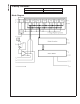
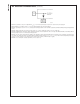
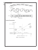
Note 7: The inputs are protected as shown below. Input voltages above V
A
or below GND will not damage this device, provided current is limited per (Note 3).
However, errors in the A/D conversion can occur if the input goes above V
A
or below GND by more than 100 mV. As an example, if V
A
is 3.3V, the full-scale input
voltage must be ≤3.4V to ensure accurate conversions.
ADC12L080
www.national.com7