
Instruction Manual
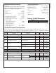
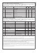

AC Electrical Characteristics (Continued)
20061007
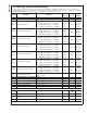
Note 8: To guarantee accuracy, it is required that |V
A
–V
D
| ≤ 100 mV and separate bypass capacitors are used at each power supply pin.
Note 9: With the test condition for V
REF
= +1.0V (2 V
P-P
differential input), the 12-bit LSB is 488 µV.
Note 10: Typical figures are at T
A
=T
J
= 25˚C, and represent most likely parametric norms. Test limits are guaranteed to National’s AOQL (Average Outgoing Quality
Level).
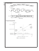
Note 11: Timing specifications are tested at TTL logic levels, V
IL
= 0.4V for a falling edge and V
IH
= 2.4V for a rising edge.
Note 12: Optimum dynamic performance will be obtained by keeping the reference input in the 0.8V to 1.5V range. The LM4051CIM3-ADJ or the LM4051CIM3-1.2
band gap voltage reference is recommended for this application.
Note 13: I
DR
is the current consumed by the switching of the output drivers and is primarily determined by load capacitance on the output pins, the supply voltage,
V
DR
, and the rate at which the outputs are switching (which is signal dependent). I
DR
=V
DR
(C
0
xf
0
+C
1
xf
1
+....C
11
xf
11
) where V
DR
is the output driver power supply
voltage, C
n
is total capacitance on the output pin, and f
n
is the average frequency at which that pin is toggling.
Note 14: Power consumption excludes output driver power. See (Note 13).
ADC12L080
www.national.com 8