
Instruction Manual

Specification Definitions
APERTURE DELAY is the time after the rising edge of the
clock to when the input signal is acquired or held for conver-
sion.
APERTURE JITTER (APERTURE UNCERTAINTY) is the
variation in aperture delay from sample to sample. Aperture
jitter manifests itself as noise in the output.
COMMON MODE VOLTAGE (V
CM
) is the d.c. potential
present at both signal inputs to the ADC.
CONVERSION LATENCY See PIPELINE DELAY.
DIFFERENTIAL NON-LINEARITY (DNL) is the measure of
the maximum deviation from the ideal step size of 1 LSB.
DUTY CYCLE is the ratio of the time that a repetitive digital
waveform is high to the total time of one period. The speci-
fication here refers to the ADC clock input signal.
EFFECTIVE NUMBER OF BITS (ENOB, or EFFECTIVE
BITS) is another method of specifying Signal-to-Noise and
Distortion or SINAD. ENOB is defined as (SINAD - 1.76) /
6.02 and says that the converter is equivalent to a perfect
ADC of this (ENOB) number of bits.
FULL POWER BANDWIDTH is a measure of the frequency
at which the reconstructed output fundamental drops 3 dB
below its low frequency value for a full scale input.
GAIN ERROR is the deviation from the ideal slope of the
transfer function. It can be calculated as:
Gain Error = Positive Full Scale Error − Offset Error
INTEGRAL NON LINEARITY (INL) is a measure of the
deviation of each individual code from a best fit straight line.
The deviation of any given code from this straight line is
measured from the center of that code value.
INTERMODULATION DISTORTION (IMD) is the creation of
additional spectral components as a result of two sinusoidal
frequencies being applied to the ADC input at the same time.
It is defined as the ratio of the power in the second and third
order intermodulation products to the power in one of the
original frequencies. IMD is usually expressed in dBFS.
MISSING CODES are those output codes that will never
appear at the ADC outputs. The ADC12L080 is guaranteed
not to have any missing codes.
NEGATIVE FULL SCALE ERROR is the difference between
the input voltage (V
IN
+−V
IN
−) just causing a transition from
negative full scale to the first code and its ideal value of 0/5
LSB.
OFFSET ERROR is the input voltage that will cause a tran-
sition from a code of 01 1111 1111 to a code of 10 0000 0000/
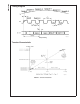
OUTPUT DELAY is the time delay after the rising edge of
the clock before the data update is presented at the output
pins.
PIPELINE DELAY (LATENCY) is the number of clock cycles
between initiation of conversion and when that data is pre-
sented to the output driver stage. Data for any given sample
is available at the output pins the Pipeline Delay plus the
Output Delay after the sample is taken. New data is available
at every clock cycle, but the data lags the conversion by the
pipeline delay.
POSITIVE FULL SCALE ERROR is the difference between
the actual last code transition and its ideal value of 1
1
⁄
2
LSB
below positive full scale.
POWER SUPPLY REJECTION RATIO (PSRR) is a mea-
sure of how well the ADC rejects a change in the power
supply voltage. PSRR1 is the ratio of the change in Full-
Scale Gain Error that results from a change in the d.c. power
supply voltage, expressed in dB. PSRR2 is a measure of
how well an a.c. signal riding upon the power supply is
rejected at the output.
SIGNAL TO NOISE RATIO (SNR) is the ratio, expressed in
dB, of the rms value of the input signal to the rms value of the
sum of all other spectral components below one-half the
sampling frequency, not including harmonics or d.c.
SIGNAL TO NOISE PLUS DISTORTION (S/N+D or SINAD)
Is the ratio, expressed in dB, of the rms value of the input
signal to the rms value of all of the other spectral compo-
nents below half the clock frequency, including harmonics
but excluding d.c.
SPURIOUS FREE DYNAMIC RANGE (SFDR) is the differ-
ence, expressed in dB, between the rms values of the input
signal and the peak spurious signal, where a spurious signal
is any signal present in the output spectrum that is not
present at the input.
TOTAL HARMONIC DISTORTION (THD) is the ratio, ex-
pressed in dBc, of the rms total of the first nine harmonic
levels at the output to the level of the fundamental at the
output. THD is calculated as
where A
f1
is the RMS power of the fundamental (output)
frequency and A
f2
through A
f10
are the RMS power in the first
9 harmonic frequencies.
Second Harmonic Distortion (2nd Harm) is the difference
expressed in dB, between the RMS power in the input
frequency at the output and the power in its 2nd harmonic
level at the output.
Third Harmonic Distortion (3rd Harm) is the difference,
expressed in dB, between the RMS power in the input
frequency at the output and the power in its 3rd harmonic
level at the output.
ADC12L080
www.national.com9