ADC14061 Self-Calibrating 14-Bit, 2.5 MSPS, 390 mW A/D Converter General Description Features The ADC14061 is a self-calibrating 14-bit, 2.5 Megasample per second analog to digital converter. It operates on a single +5V supply, consuming just 390mW (typ). n n n n The ADC14061 provides an easy and affordable upgrade from 12 bit converters. The ADC14061 may also be used to replace many hybrid converters with a resultant saving of space, power and cost.
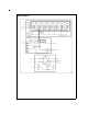
Block Diagram DS100103-2 www.national.
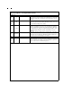
Pin Descriptions and Equivalent Circuits Pin No. Symbol Equivalent Circuit Description Analog I/O 1 VIN+ Non-Inverting analog signal Input. With a 2.0V reference voltage and a 2.0V common mode voltage, VCM, the input signal voltage range is from 1.0 volt to 3.0 Volts. 4 VIN− Inverting analog signal Input. With a 2.0V reference voltage and a 2.0V common mode voltage, VCM, the input signal voltage range is from 1.0 Volt to 3.0 Volts. The input signal should be balanced for best performance.
Pin Descriptions and Equivalent Circuits (Continued) Digital I/O Clock Digital clock input. The range of frequencies for this input is 300 kHz to 2.5 MHz. The clock frequency should not be changed or interrupted during conversion or while reading data output. 11 CAL CAL is a level-sensitive digital input that, when pulsed high for at least two clock cycles, puts the ADC into the CALIBRATE mode.
Pin Descriptions and Equivalent Circuits (Continued) Digital Power Positive digital supply pin. This pin should be connected to the same clean, quiet +5V source as is VA and bypassed to DGND with a 0.1 µF monolithic capacitor in parallel with a 10µF capacitor, both located within 1 cm of the power pin. 20 VD 12,13 14,19, 41,42, 43 DGND The ground return for the digital supply. AGND and DGND should be connected together directly beneath the ADC14061 package.
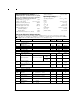
Absolute Maximum Ratings (Note 1) Storage Temperature If Military/Aerospace specified devices are required, please contact the National Semiconductor Sales Office/ Distributors for availability and specifications. Operating Ratings(Notes 1, 2) Operating Temperature Range 0˚C ≤ TA ≤ +70˚C −0.3V to V+ +0.3V VA, VD +4.75V to +5.25V ± 25mA ± 50mA VD I/O Supply Voltage (VA, VD, VD I/O) Voltage on Any I/O Pin −65˚C to +150˚C 6.
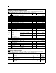
DC and Logic Electrical Characteristics The following specifications apply for AGND = DGND = DGND I/O = 0V, V+ = VA = VD = +5.0V, VD I/O = 3.0V or 5.0V, PD = +5V, VREF+ = +2.0V, VREF IN = AGND, fCLK = 2.5 MHz, RS = 25Ω, CL = 50 pF/pin. After Auto-Cal @ Temperature. Boldface limits apply for TA = TJ = TMIN to TMAX: all other limits TA = TJ = 25˚C(Notes 7, 8, 9) Symbol Parameter Conditions Typical (Note 10) CLOCK, RD, PD Digital Input Characteristics VIN(1) Logical ″1″ Input Voltage V+ = 5.
AC Electrical Characteristics (Continued) The following specifications apply for AGND = DGND = DGND I/O = 0V, V+ = VA = VD = +5.0V, VD I/O = 3.0V or 5.0V, PD = +5V, VREF+ = +2.0V, VREF IN = AGND, fCLK = 2.5 MHz, RS = 25Ω, CL = 50 pF/pin. After Auto-Cal @ Temperature.
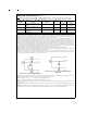
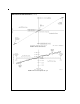
AC Electrical Characteristics (Continued) DS100103-13 FIGURE 1. Transfer Characteristics DS100103-14 FIGURE 2. Errors removed by Auto-Cal cycle 9 www.national.
Typical Performance Characteristics INL vs Temperature DNL vs Temperature DS100103-25 INL vs VREF and Temperature DS100103-26 DNL vs VREF DS100103-27 THD vs Temperaure DS100103-35 SINAD & ENOB vs Temperature SNR vs Temperature DS100103-28 DS100103-34 SINAD & ENOB vs Clock Duty Cycle SFDR vs Temperature DS100103-29 DS100103-30 IMD Spectral Response DS100103-32 www.national.
INTEGRAL NON-LINEARITY (INL) is a measure of the deviation of each individual code from a line drawn from negative full scale (1⁄2 LSB below the first code transition) through positive full scale (the last code transition). The deviation of any given code from this straight line is measured from the center of that code value. PIPELINE DELAY (LATENCY) is the number of clock cycles between initiation of conversion and the availability of that same conversion result at the output.
Timing Diagrams (Continued) DS100103-16 TIMING DIAGRAM 2. Reset and Calibration www.national.
Functional Description VREF (MID) is the reference mid-point and is derived from VCM. This point is brought out only to be by passed. By pass this pin with 0.1µF capacitor to ground. Do not load this pin. Operating on a single +5V supply, the ADC14061 uses a pipelined architecture and has error correction circuitry and a calibration mode to help ensure maximum performance at all times.
Applications Information Note that the buffer used for this purpose should be a slow, low noise amplifier. The LMC660, LMC662, LMC272 and LMC7101 are good choices for driving the VCM pin of the ADC14061. (Continued) The sign bit of the output word will be a logic low when VIN+ is greater than VIN− . When VIN+ is less than VIN−, the sign bit of the output word will be a logic high. 2.0 DIGITAL INPUTS Digital Inputs consist of CLOCK, RESET, CAL, RD and PD. 2.
Applications Information 4.0 POWER SUPPLY CONSIDERATIONS Each power supply pin should be bypassed with a parallel combination of a 10 µF capacitor and a 0.1 µF ceramic chip capacitor. The chip capacitors should be within 1⁄2 centimeter of the power pins. Leadless chip capacitors are preferred because they provide low lead inductance. (Continued) To avoid signal clipping and distortion, VREF+ OUT should not exceed 3.3V, VREF− OUT should not be below 750 mV and VCM should be held in the range of 1.8V to 2.
Applications Information (Continued) DS100103-20 FIGURE 7. Differential drive circuit of Figure 6. All 5k resistors are 0.1%. Tolerance of the other resistors is not critical. DS100103-22 FIGURE 8. Driving the signal inputs with a transformer. www.national.
Applications Information rest of the ground plane. A typical width is 3/16 inch (4 to 5 mm).This narrowing beneath the converter provides a fairly high impedance to the high frequency components of the digital switching currents, directing them away from the analog pins. The relatively lower frequency analog ground currents see a relatively low impedance across this narrow ground connection. (Continued) 5.
Applications Information (Continued) DS100103-23 FIGURE 9. Example at a suitable layout. 7.0 COMMON APPLICATION PITFALLS Driving the inputs (analog or digital) beyond the power supply rails. For proper operation, all inputs should not go more than 100 mV beyond the supply rails (more than 100 mV below the ground pins or 100 mV above the supply pins). Exceeding these limits on even a transient basis may cause faulty or erratic operation. It is not uncommon for high speed digital circuits (e.g.
Applications Information 1.8V ≤ VREF ≤ 2.2V with VREF− IN ≤ 1.0V. Operating outside of these limits could lead to signal distortion. Using a clock source with excessive jitter, using excessively long clock signal trace, or having other signals coupled to the clock signal trace. This will cause the sampling interval to vary, causing excessive output noise and a reduction in SNR performance. (Continued) put alternates between 12 pF and 28 pF, depending upon the phase of the clock.
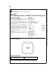
ADC14061 Self-Calibrating 14-Bit, 2.5 MSPS, 390 mW A/D Converter Physical Dimensions inches (millimeters) unless otherwise noted 52-Lead Thin Quad Flat Pack Ordering Information Package ADC14061CCVT NS Package Number VEG52A LIFE SUPPORT POLICY NATIONAL’S PRODUCTS ARE NOT AUTHORIZED FOR USE AS CRITICAL COMPONENTS IN LIFE SUPPORT DEVICES OR SYSTEMS WITHOUT THE EXPRESS WRITTEN APPROVAL OF THE PRESIDENT OF NATIONAL SEMICONDUCTOR CORPORATION. As used herein: 2.