
Owner's manual
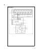
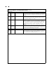

Pin Descriptions and Equivalent Circuits (Continued)
Digital I/O
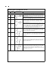
10 Clock
Digital clock input. The range of frequencies for this input is 300 kHz to 2.5
MHz. The clock frequency should not be changed or interrupted during
conversion or while reading data output.
11 CAL
CAL is a level-sensitive digital input that, when pulsed high for at least two
clock cycles, puts the ADC into the CALIBRATE mode. Calibration should
be performed upon ADC power-up (after asserting a reset) and each time
the temperature changes by more than 50˚C since the ADC14061 was last
calibrated. See Section 2.3 for more information.
40 RESET
RESET is a level-sensitive digital input that, when pulsed high for at least 2
CLOCK cycles, results in the resetting of the ADC. This reset pulse must
be applied after ADC power-up, before calibration.
18 RD
RD is the (READ) digital input that, when low, enables the output data
buffers. When this input pin is high, the output data bus is in a high
impedance state.
44 PD
PD is the Power Down input that, when low, puts the converter into the
power down mode. When this pin is high, the converter is in the active
mode.
17 EOC
EOC is a digital output that, when low, indicates the availability of new
conversion results at the data output pins.
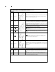
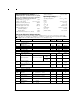
23-32
35-38
D00-13
Digital data outputs that make up the 14-bit TRI-STATE conversion results.
D00 is the LSB, while D13 is the MSB (SIGN bit) of the two’s complement
output word.
Analog Power
6, 7,
45
V
A
Positive analog supply pins. These pins should be connected to a clean,
quiet +5V source and bypassed to AGND with 0.1 µF monolithic capacitors
in parallel with 10 µF capacitors, both located within 1 cm of these power
pins.
5, 8,
46
AGND
The ground return for the analog supply. AGND and DGND should be
connected together directly beneath the ADC14061 package. See Section
5 (Layout and grounding) for more details).
www.national.com 4