
Owner's manual
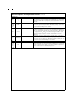

Absolute Maximum Ratings (Note 1)
If Military/Aerospace specified devices are required,
please contact the National Semiconductor Sales Office/
Distributors for availability and specifications.
Supply Voltage (V
A
,V
D
,V
D
I/O) 6.5V
Voltage on Any I/O Pin −0.3V to V
+
+0.3V
Input Current at Any Pin (Note 3)
±
25mA
Package Input Current (Note 3)
±
50mA
Power Dissipation at T
A
=
25˚C (Note 4)
ESD Susceptibility (Note 5)
Human Body Model 1500V
Machine Model 200V
Soldering Temp., Infrared, 10 sec. (Note 6) 300˚C
Storage Temperature −65˚C to +150˚C
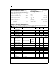
Operating Ratings(Notes 1, 2)
Operating Temperature
Range
0˚C ≤ T
A
≤ +70˚C
V
A,
V
D
+4.75V to +5.25V
V
D
I/O 2.7V to V
D
V
REF
− IN 1.0V to 3.0V
V
REF
− IN AGND to 0.1V
Digital Inputs −0.05V to V
D
+ 0.05V
|V
A
−V
D
| ≤100 mV
|AGND - DGND | 0V to 100 mV
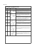
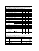
Converter Electrical Characteristics
The following specifications apply for AGND
=
DGND
=
DGND I/O
=
0V, V
+
=
V
A
=
V
D
=
+5.0V, V
D
I/O
=
3.0V or 5.0V,
PD
=
+5V, V
REF+ IN
=
+2.0V, V
REF− IN
=
AGND, f
CLK
=
2.5 MHz, C
L
=
50 pF/pin. After Auto-Cal
@
Temperature. Boldface
limits apply for T
A
=
T
J
=
T
MIN
to T
MAX
: all other limits T
A
=
T
J
=
25˚C(Notes 7, 8, 9)
Symbol Parameter Conditions
Typical
(Note 10)
Limits
(Note 11)
Units
Static Converter Characteristics
Resolution with No
Missing Codes
14 Bits(min)
INL Integral Non Linearity
±
0.75
±
2.5 LSB(max)
DNL Differential Non Linearity
±
0.3
±
1.0 LSB(max)
Full-Scale Error
±
0.4
±
2.8
%
FS(max)
Zero Offset Error +0.1
±
0.6
%
FS(max)
Reference and Analog Input Characteristics
V
IN
Input Voltage Range
(V
IN+
−V
IN−
)
V
REF
=
V
REF
+
IN
−V
REF
+
IN
− 2.0
1.8
2.2
V(min)
V(max)
C
IN
Input Capacitance V
IN
=
1.0V + 0.7Vrms
(CLK
LOW)
12 pF
(CLK
HIGH)
28 pF
V
REF
Reference Voltage
Range [( V
REF
+
IN
)−
(V
REF
−
IN
)] (Note 14)
2.00
1.8
2.2
V(min)
V(max)
Reference Input
Resistance
3.5 KΩ
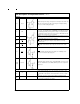
Dynamic Converter Characteristics
BW Full Power Bandwidth 8 MHz
SNR Signal-to-Noise Ratio f
IN
=
500 kHz, V
IN
=
1.9V
P-P
80 dB
SINAD
Signal-to-Noise &
Distortion
f
IN
=
500 kHz, V
IN
=
1.9V
P-P
79 dB
ENOB Effective Number of Bits f
IN
=
500 kHz, V
IN
=
1.9V
P-P
12.8 Bits
THD
Total Harmonic
Distortion
f
IN
=
500 kHz, V
IN
=
1.9V
P-P
−88 dB
SFDR
Spurious Free Dynamic
Range
f
IN
=
500 kHz, V
IN
=
1.9V
P-P
90 dB
IMD
Intermodulation
Distortion
f
IN1
=
95 kHz
f
IN2
=
105 kHz
−97 dB
www.national.com 6