
Manual
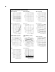

AC Electrical Characteristics (Continued)
The following specifications apply for AGND
=
DGND
=
DGND I/O
=
0V, V
+
=
V
A
=
V
D
=
+5.0V, V
D
I/O
=
3.0V or 5.0V,
PD
=
+5V, V
REF
+
=
+2.0V, V
REF IN
=
AGND, f
CLK
=
2.5 MHz, RS
=
25Ω,C
L
=
50 pF/pin. After Auto-Cal. Boldface limits
apply for T
A
=
T
J
=
T
MIN
to T
MAX
: all other limits T
A
=
T
J
=
25˚C(Notes 7, 8, 9)
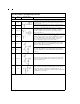
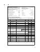
Symbol Parameter Conditions
Typical
(Note 10)
Limits
(Note 11)
Units
(Limits)
t
EOCL
Falling edge of CLK to falling
edge of EOC
1/(4f
CLK
)
90
130
ns(min)
ns(max)
t
DATA_VALID
Falling edge of CLOCK to Data
Valid
1/(8f
CLK
)
38
95
ns(min)
ns(max)
t
ON
RD low to data valid on D00
-D15
23 33 ns(max)
t
OFF
RD high to D00 -D15 in
TRI-STATE
25 33 ns(max)
t
CAL
Calibration Time 110 ms
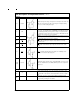
Note 1: Absolute Maximum Ratings indicate limits beyond which damage to the device may occur. Operating Ratings indicate conditions for which the device is func-
tional, but do not guarantee specific performance limits. For guaranteed specifications and test conditions, see the Electrical Characteristics. The guaranteed speci-
fications apply only for the test conditions listed. Some performance characteristics may degrade when the device is not operated under the listed test conditions.
Note 2: All voltages are measured with respect to GND
=
AGND
=
DGND I/O
=
0V, unless otherwise specified.
Note 3: When the input voltage at any pin exceeds the power supplies (that is, V
IN
<
AGND or V
IN
>
V
A
or V
D
), the current at that pin should be limited to 25 mA.
The 50 mA maximum package input current rating limits the number of pins that can safely exceed the power supplies with an input current of 25 mA to two.
Note 4: The absolute maximum junction temperature (T
J
max) for this device is 150˚C. The maximum allowable power dissipation is dictated by TJmax, the
junction-to-ambient thermal resistance (θ
JA
), and the ambient temperature (T
A
), and can be calculated using the formula P
D
MAX=(T
J
max - T
A
)/θ
JA
. In the 52-pin
TQFP, θ
JA
is 70˚C/W, so P
D
MAX = 1,785 mW at 25˚C and 1,142 mW at the maximum operating ambient temperature of 70˚C. Note that the power dissipation of this
device under normal operation will typically be about 416 mW (390 mW quiescent power + 26 mW due to 1 TTL load on each digital output. The values for maximum
power dissipation listed above will be reached only when the ADC16061 is operated in a severe fault condition (e.g. when input or output pins are driven beyond the
power supply voltages, or the power supply polarity is reversed). Obviously, such conditions should always be avoided.
Note 5: Human body model is 100 pF capacitor discharged through a 1.5kΩ resistor. Machine model is 220 pF discharged through ZERO Ω.
Note 6: See AN450, ″Surface Mounting Methods and Their Effect on Product Reliability″, or the section entitled ″Surface Mount″ found in any post 1986 National
Semiconductor Linear Data Book, for other methods of soldering surface mount devices.
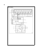
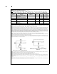
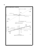
Note 7: The inputs are protected as shown below. Input voltages above V
A
or below GND will not damage this device, provided current is limited per Note 3. How-
ever, errors in the A/D conversion can occur if the input goes above V
A
or below GND by more than 100 mV. As an example, if V
A
is 4.75 V
DC
, the full-scale input
voltage must be ≤4.85V
DC
to ensure accurate conversions
Note 8: To guarantee accuracy, it is required that V
A
and V
D
be connected together and to the same power supply with separate bypass capacitors at each V
+
pin.
Note 9: With the test condition for V
REF
=
(V
REF
+)−(V
REF
−) given as +2.0V, the 16-bit LSB is 30 µV.
Note 10: Typical figures are at T
A
=
T
J
=
25˚C, and represent most likely parametric norms.
Note 11: Tested limits are guaranteed to Nationsl’s AOQL (Average Outgoing Quality Level) with 50
%
duty cycle clock.
Note 12: Integral Non Linearity is defined as the deviation of the analog value, expressed in LSBs, from the straight line that passes through positive full-scale and
negative full-scale.
Note 13: Timing specifications are tested at the TTL logic levels, V
IL
=
0.4V for a falling edge and V
IH
=
2.4V for a rising edge. TRI-STATE output voltage is forced
to 1.4V.
Note 14: Optimum SNR performance will be obtained by keeping the reference voltage in the 1.8V to 2.2V range. The LM4041CIM3-ADJ (SOT-23 package), or the
LM4041CIZ-ADJ (TO-92 package), bandgap voltage reference is recommended for this application.
DS100889-11
ESD Protection Scheme for Digital Input pins
DS100889-12
ESD Protection Scheme for Analog Input and Digital
Output pins
www.national.com 8