Integrated Circuits Inc. aP89341/170/085 A PLUS MAKE YOUR PRODUCTION A-PLUS VOICE OTP IC aP89341 – 341sec aP89170 – 170sec aP89085 – 85sec APLUS INTEGRATED CIRCUITS INC. Address: 3 F-10, No. 32, Sec. 1, Chenggung Rd., Taipei, Taiwan 115, R.O.C. (115)台北市南港區成功路一段 32 號 3 樓之 10. Sales E-mail: sales@aplusinc.com.tw TEL: 886-2-2782-9266 FAX: 886-2-2782-9255 WEBSITE : http: //www.aplusinc.com.tw Support E-mail: service@aplusinc.com.
Integrated Circuits Inc. aP89341/170/085 FEATURES • Standard CMOS process. • Embedded 8M/4M/2M EPROM. • 341/170/85 sec Voice Length at 6KHz sampling and 4-bit ADPCM compression. • Maximum 254 voice groups. • Combination of voice blocks to extend playback duration. • 7680 table entries are available for voice block combinations.
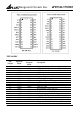
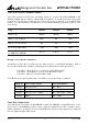
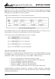
Integrated Circuits Inc. aP89341/170/085 PIN NAMES PIN (24-pin) Playback Mode 1 2 3 4 5 6 7 8 9 10 11 12 13 14 15 16 17 18 19 ~ 24 S7 S8 VSS VOUT1 VOUT2 VDD AVDD VPP OSC COUT AVSS OUT3 OUT2 OUT1 RST SBT M1 M0 S1~S6 Ver 2.
Integrated Circuits Inc. aP89341/170/085 PIN DESCRIPTIONS S1 ~ S8 Input Trigger Pins: - In Key Trigger Mode, S1 to S8 is used to trigger the first 32 out of the total 254 Voice Groups . - In CPU Parallel Command Mode, S1 to S8 serve as Voice Group address inputs for 254 Voice Groups with S1 as LSB and S8 as MSB. - In CPU Serial Command Mode, S1 is Chip Select (SC) pin to initiate the command input. S2 is the Serial Clock (SCK) pin which clocks the input command and data bits into the chip.
Integrated Circuits Inc. aP89341/170/085 VOICE SECTION COMBINATIONS Voice files created by the PC base developing system are stored in the built-in EPROM of the aP89341/170/085 chip as a number of fixed length Voice Blocks. Voice Blocks are then selected and grouped into Voice Groups for playback. Up to 254 Voice Groups are allowed. A Voice Block Table is used to store the information of combinations of Voice Blocks and then group them together to form Voice Group.
Integrated Circuits Inc. aP89341/170/085 Programmable Options In Key Trigger Mode (M1=0; M0=0) and CPU Parallel Trigger Mode (M1=0; M0=1), user can select different trigger functions and output signals to be sent out from the pins OUT1, OUT2 and OUT3. Options that affect all Voice Group playback are called Whole Chip Options. Options that only affect the playback of individual Voice Group are called Group Options. Whole Chip Options • Long (16ms) or short (65us) debounce time at 8KHz sampling rate.
Integrated Circuits Inc. aP89341/170/085 Group Options User selectable options that affect each individual group are called Group Options. They are: • • • • Edge or Level trigger Unholdable or Holdable trigger Re-triggerable or non-retriggerable Stop pulse disable or enable Fig. 4 to Fig. 9 show the voice playback with different combination of triggering mode and the relationship between outputs and voice playback. Fig. 4 Level, Unholdable, Non-retriggerable Fig. 5 Level Holdable Fig.
Integrated Circuits Inc. aP89341/170/085 Fig. 7 Edge, Unholdable, Non-retrigger Fig. 8 Edge, Holdable Fig. 9 SBT sequential trigger with Edge Holdable and Unholdable TRIGGER MODES There are three trigger modes available for aP89341/170/085 series which are determined by setting M1 and M2 pins to logic HIGH or LOW. • • • Ver 2.
Integrated Circuits Inc. aP89341/170/085 Key Trigger Mode (M1=0, M0=0) With this trigger mode, the beginning 32 Voice Groups are triggered by setting S1 to S8 to HIHG or LOW in different combinations. Each Voice Group can have its only independent trigger options (See Fig. 4, 5, 7 and 8 for trigger options definition). A maximum of 254 Voice Groups are available. The 33rd to 254th Voice Groups can only be triggered one by one sequentially with the SBT key (See Fig. 6 and 9).
Integrated Circuits Inc. aP89341/170/085 CPU Parallel Trigger Mode (M1=0, M0=1) In this mode, S8 to S1 serve as 8-bit addresses input for 254 Voice Groups with S8 represents the MSB and S1 represents LSB. After Group address is set and ready, setting the SBT input pin to HIGH will trigger the corresponding Voice Group to playback. Trigger options defined in Fig. 4, 5, 7 and 8 are valid for this mode. Fig.
Integrated Circuits Inc.
Integrated Circuits Inc. • aP89341/170/085 Power-down with RAMP-DOWN (PD2-A9H) or without RAMP-DOWN (PD1-E1H) Fig. 12 Power-down commands timing 1. 2. 3. 4. 5. • PDN1 will power-down the chip and set the COUT data to 00H immediately. PDN2 will power-down the chip by Ramp-down the COUT from its current value to 00H. Power-down will start after 350us (at 6KHz sampling rate). The OUT1 pin (BUSY) will output logic HIGH during Ramp-down operation.
Integrated Circuits Inc. aP89341/170/085 1. Signal output from the pin, OUT2, is defined by G[3:0], as below: G[3:0] 000 001 010 011 2. 3. 4. 5. • OUT2 BUSYB 8KHz 4KHz 2KHz G[3:0] 100 101 110 111 OUT2 1KHz 16Hz 1MHz FULLB If the STATUS is not executed, default value of OUT2 is the internal Reset signal. BUSYB is the logical inversion of BUSY. EMPTY (or FULLB) is the logical inversion of FULL. Only the 1MHz clock will not be stopped by the PAUSE command. Pause and Resume (PLAUS-39H; RESUME-1DH) Fig.
Integrated Circuits Inc. aP89341/170/085 BLOCK DIAGRAM Fig. 17 Block Diagram ABSOLUTE MAXIMUM RATINGS Symbol Rating Unit VDD - VSS -0.5 ~ +3.8 V VIN VSS - 0.3
Integrated Circuits Inc. aP89341/170/085 DC CHARACTERISTICS ( TA = 0 to 70℃, VDD = 3.3V, VSS = 0V ) Symbol Parameter Min. Typ. Max. Unit Condition VDD Operating Voltage 2.2 3.0 3.6 V ISB Standby current 1 5 μA I/O open IOP Operating current 15 mA I/O open VIH "H" Input Voltage 2.5 3.0 3.5 V VDD=3.0V VIL "L" Input Voltage -0.3 0 0.5 V VDD=3.0V IOL VOUT low O/P Current 120 mA Vout=0.3V IOH VOUT high O/P Current -65 mA Vout=2.
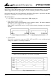
Integrated Circuits Inc. aP89341/170/085 TIMING WAVEFORMS KEY Trigger Mode tKD S1~S8, SBT tSTPD COUT STOP tSTPW BUSY tBH tBD CPU Parallel Mode tAS Addr. S1~S8 SBT tAH tSBTW CPU Serial Command Mode tCH tCS S1(CS) tDH S3(DI) tCOUTD tSCKW S2(SCK) COUT tDS tBH tSCKC tBD BUSY FULL tFD Fig. 18 Timing Waveform Ver 2.
Integrated Circuits Inc. aP89341/170/085 AC CHARACTERISTICS ( TA = 0 to 70℃, VDD = 3.3V, VSS = 0V, 8KHz sampling ) Symbol Parameter Min. Typ. Max.
Integrated Circuits Inc. aP89341/170/085 OSCILLATOR RESISTANCE TABLE Sampling Frequency KHz 4.90 5.26 5.88 6.09 6.33 6.67 6.85 7.14 7.46 7.70 8.06 8.47 8.93 9.26 9.80 10.42 ROSC KOhm ROSC KOhm 140 130 120 110 100 91 82 75 68 62 56 51 43 300 290 280 270 260 250 240 230 220 210 200 190 180 170 160 150 Sampling Frequency KHz 11.00 11.76 12.50 13.33 14.51 15.63 16.95 18.18 19.23 20.83 22.22 23.81 25.00 Note: The data in the above tables are within 3% accuracy and measured at VDD = 3.0V.
Integrated Circuits Inc. aP89341/170/085 TYPICAL APPLICATIONS Key Trigger Mode 0.1uF 0.01uF 8Ω Speaker VDD, AVDD,VPP RST ROSC 390Ω S1 S2 S3 • • 3.3V • • • 8050D COUT OSC VOUT1 VOUT2 • S8 SBT 8 / 16Ω Speaker OUT1 VSS, AVSS Fig. 22 Using 3.3V Battery HT7335 10uF 0.01uF VDD, AVDD,VPP ROSC RST • • • S1 S2 S3 • • VOUT1 VOUT2 • S8 SBT Output driving of HT LDO: HT7136 (30mA, 3.6V) HT7133 (30mA, 3.3V) HT7536 (100mA, 3.6V) HT7335 (250mA, 3.5V) 8050D COUT OSC 4.
Integrated Circuits Inc. aP89341/170/085 CPU Parallel Mode VIN=+5V VOUT=+3.5V HT7335 10uF 0.01uF ROSC VDD, AVDD,VPP RST OSC MCU Addr[0] Addr[1] Addr[2] • • • 8050D S1 S2 S3 • • • • • • Addr[7] I[0..2] COUT 8Ω Speaker S8 Rin 3 OUT[1..3] VSS, AVSS Rin = 860KΩ x (VIN-VOUT) / VIN Fig. 24 5V CPU Control with COUT Ver 2.
Integrated Circuits Inc. aP89341/170/085 CPU Serial Command Mode VIN=+5V VOUT=+3.5V HT7335 10uF 0.01uF ROSC VDD, AVDD,VPP RST OSC 10uF 2 COUT Rin S1 (CS) S2 (SCK) S3 (DI) 10KΩ 33Ω 10u BUSY FULL 8Ω Speaker Vcc 7 + 8 - 6 + OUT1 5 OUT3 - 1 TDA2822M MCU CS SCK DI 3 0.1u Gnd 0.01uF 4.7Ω 4 VSS, AVSS 0.1u 4.7Ω Rin = 860KΩ x (VIN-VOUT) / VIN Fig. 25 5V CPU Control with TDA Power Amplifier Ver 2.
Integrated Circuits Inc. aP89341/170/085 BONDING PAD DIAGRAMS aP89341 Notes: 1. 2. 3. 4. Ver 2.1 Two VPP pads should be connected to the Positive Power Supply during voice playback. VDD and AVDD should be connected to the Positive Power Supply. VSS and AVSS should be connected to the Power GND. Substrate should be connected to the Power GND.
Integrated Circuits Inc. aP89341/170/085 aP89170 aP89085 Notes: 5. 6. 7. 8. Ver 2.1 VPP and VSL pads should be connected to the Positive Power Supply during voice playback. VDD and AVDD should be connected to the Positive Power Supply. VSS and AVSS should be connected to the Power GND. Substrate should be connected to the Power GND.
Integrated Circuits Inc. aP89341/170/085 PACKAGES DIMENSION OUTLINES 24-Pin 300mil P-DIP Package 28-Pin 300mil SOP Package Ver 2.