
Instruction Manual


Integrated Circuits Inc. aP8921A/10A
Ver 2.0 Dec 6, 2006
3
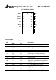
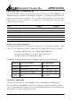
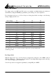
PIN NAMES
PIN
Playback
Mode
OTP Program
Mode
Description
1 OUT1 OEB Programmable output (I/O pin)
2 VOUT1 - PWM output to drive speaker directly
3 VOUT2 - PWM output to drive speaker directly
4 VSS VSS Power Ground
5 OUT2 IO Programmable output (I/O pin)
6 V33 V33 Power Supply for OTP programming
7 COUT - D/A current output
8 OSC ACLK Oscillator input
9 VPP VPP Supply voltage for OTP programming
10 S1 S1 Trigger pin (input with internal pull-down)
11 S2 S2 Trigger pin (input with internal pull-down)
12 VDD VDD 2.6 – 5.0V Positive Power Supply
13 S3 S3 Trigger (input with internal pull-down)
14 S4 S4 Trigger (input with internal pull-down)
15 SBT PGM Trigger pin (input with internal pull-down)
16 RST DCLK Reset pin (input with internal pull-down)
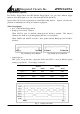
PIN CONFIGURATIONS
1
2
3
4
5
6
7
8
16
15
14
13
12
11
10
9
OUT1
VOUT1
VOUT2
VSS
OUT2
V33
COUT
OSC
VPP
VDD
S1
S2
S3
S4
SBT
RST