
Manual
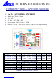

INTEGRATED CIRCUITS INC.
http://www.aplusinc.com.tw PAGE / 5 VER1.3
4
3FE1 System Control 1. Write only
Bit 0: = 1 -(Timer A clock selects system clock.)
0- (Timer A clock selects 32.768k Hz.) (Default)
1: = not used (must be 0.)
2: = 1-- (Timer A enabled)
0 --(Timer A disabled) (Default)
3: = 1 -- (Timer B enabled)
0-- (Timer B disabled) (Default)
4: = 1--(Timer A interrupt enabled)
0-- (Timer A interrupt disabled) (Default)
5: = 1-- (Timer B NMI enabled)
0 --(Timer B NMI disabled) (Default)
6: = 1-- (System clock = 32768Hz)
0-- (System clock = PLL clock) (Default)
7: = 1-- (Watchdog timer enabled) (Default)
0-- (Watchdog timer disabled)
3FE2 System control 2. Write only
Bit 0: = 1-- (Entry to stand-by mode)
In stand-by mode, CPU is held. The NMI and
IRQ will wake up the CPU.
1: = 1 --(Entry to sleep mode)
In sleep mode, both of the main system clock
and 32768Hz will be stopped, so all functions
are stopped and only an external interrupt can
wake up this chip.
3-2: = 00 (system clock = Fxosc/2 X 256 (4.19MHz)) (Default)
01 (system clock = Fxosc/2 X 512 (8.38MHz))
10 (system clock = Fxosc/2 X 768 (12.58MHz))
7-4: = 0xxx (Fix-timer disabled)
1000 (Fix-timer = 64Hz)
1001 (Fix-timer = 32Hz)
1010 (Fix-timer = 16Hz)
1011 (Fix-timer = 8Hz)
1100 (Fix-timer = 4Hz)
1101 (Fix-timer = 2Hz)
1110 (Fix-timer = 1Hz)
1111 (Fix-timer = 0.5Hz)
3FE3 interrupt enable register of Port_a[7..0]. Write only
A ‘0’ in this register will set the interrupt function of the corresponding pin of port_a to be enabled.
The default value for each bit is ‘1’.
3FE4 data register of Port_a[7..0]. Read and write
3FE5 direction register of Port_a[7..0]. Write only
A ‘1’ in this register will set the corresponding pin of port_a to be output. The
default value for each bit is zero.
3FE6 data register of Port_b[7..0]. Write only
3FE7 Clear watchdog timer. Write only
The watchdog timer reset will happen if the programmer does not clear the
watchdog timer before watchdog timer time-out occurs.
3FE8 Low byte of voice channel 0. Write only
Bit 2-0: Reserved.
Bit 3: not used (must be 0.)
Bit 7-4: = low nibble byte of voice channel 0
3FE9 high byte of voice channel 0. Write only
The resolution of voice channel 0 is 12 bits ($3FE9,$3FE8 bit7_4).
3FEA Bank register for coprocessor. Write only
3FEB Bank register MSB bit for coprocessor. Write only
Bank register is a 9-bit register ($3FEB bit0 and $3FEA bit7-0).
The memory range of bank is from $4000 to $7FFF.
Bit 7-1: Reserved.
3FEC, 3FED Timer A data or tone0 generator. Read and write. After timer_a is enabled,
the timer will start to count down. When timer counts to zero, the timer will count from the
initial value and timer_a IRQ will happen.
The time elapsing = (($3FED,$3FEC)+1) / (Timer A input clock)