
Owner's manual


1
Features
• Low-voltage and Standard-voltage Operation
–2.7(V
CC
=2.7Vto5.5V)
–1.8(V
CC
=1.8Vto5.5V)
• Internally Organized 128 x 8 (1K), 256 x 8 (2K), 512 x 8 (4K),
1024 x 8 (8K) or 2048 x 8 (16K)
• 2-wire Serial Interface
• Schmitt Trigger, Filtered Inputs for Noise Suppression
• Bi-directional Data Transfer Protocol
• 100 kHz (1.8V, 2.5V, 2.7V) and 400 kHz (5V) Compatibility
• Write Protect Pin for Hardware Data Protection
• 8-byte Page (1K, 2K), 16-byte Page (4K, 8K, 16K) Write Modes
• PartialPageWritesareAllowed
• Self-timed Write Cycle (10 ms max)
• High-reliability
– Endurance: 1 Million Write Cycles
– Data Retention: 100 Years
• Automotive Grade and Extended Temperature Devices Available
• 8-lead PDIP, 8-lead JEDEC SOIC, 8-lead MAP and 8-lead TSSOP Packages
Description
The AT24C01A/02/04/08/16 provides 1024/2048/4096/8192/16384 bits of serial elec-
trically erasable and programmable read-only memory (EEPROM) organized as
128/256/512/1024/2048 words of 8 bits each. The device is optimized for use in many
industrial and commercial applications where low-power and low-voltage operation
are essential. The AT24C01A/02/04/08/16 is available in space-saving 8-pin PDIP,
8-lead JEDEC SOIC, 8-lead MAP and 8-lead TSSOP packages and is accessed via a
2-wire serial interface. In addition, the entire family is available in 2.7V (2.7V to 5.5V)
and 1.8V (1.8V to 5.5V) versions.
2-wire
Serial EEPROM
1K(128x8)
2K(256x8)
4K(512x8)
8K (1024 x 8)
16K (2048 x 8)
AT24C01A
AT24C02
AT24C04
AT24C08
AT24C16
Rev. 0180I–SEEPR–10/02
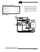
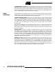
Pin Configurations
Pin Name Function
A0 - A2 Address Inputs
SDA Serial Data
SCL Serial Clock Input
WP Write Protect
NC No Connect
8-lead SOIC
1
2
3
4
8
7
6
5
A0
A1
A2
GND
VCC
WP
SCL
SDA
8-pin PDIP
1
2
3
4
8
7
6
5
A0
A1
A2
GND
VCC
WP
SCL
SDA
8-lead TSSOP
1
2
3
4
8
7
6
5
A0
A1
A2
GND
VCC
WP
SCL
SDA
8-lead MAP
Bottom View
1
2
3
4
8
7
6
5
VCC
WP
SCL
SDA
A0
A1
A2
GND