
Owner's manual


4
AT24C01A/02/04/08/16
0180I–SEEPR–10/02
Note: 1. This parameter is characterized and is not 100% tested.
Note: 1. V
IL
min and V
IH
max are reference only and are not tested.
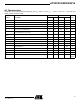
Pin Capacitance
(1)
Applicable over recommended operating range from T
A
=25°C, f = 1.0 MHz, V
CC
= +1.8V.
Symbol Test Condition Max Units Conditions
C
I/O
Input/Output Capacitance (SDA) 8 pF V
I/O
=0V
C
IN
Input Capacitance (A
0
,A
1
,A
2
,SCL) 6 pF V
IN
=0V
DC Characteristics
Applicable over recommended operating range from: T
AI
=-40°Cto+85° C, V
CC
= +1.8V to +5.5V, T
AC
=0°Cto+70°C,
V
CC
= +1.8V to +5.5V (unless otherwise noted).
Symbol Parameter Test Condition Min Typ Max Units
V
CC1
Supply Voltage 1.8 5.5 V
V
CC2
Supply Voltage 2.5 5.5 V
V
CC3
Supply Voltage 2.7 5.5 V
V
CC4
Supply Voltage 4.5 5.5 V
I
CC
Supply Current V
CC
= 5.0V READ at 100 kHz 0.4 1.0 mA
I
CC
Supply Current V
CC
= 5.0V WRITE at 100 kHz 2.0 3.0 mA
I
SB1
Standby Current V
CC
=1.8V V
IN
=V
CC
or V
SS
0.6 3.0 µA
I
SB2
Standby Current V
CC
=2.5V V
IN
=V
CC
or V
SS
1.4 4.0 µA
I
SB3
Standby Current V
CC
=2.7V V
IN
=V
CC
or V
SS
1.6 4.0 µA
I
SB4
Standby Current V
CC
=5.0V V
IN
=V
CC
or V
SS
8.0 18.0 µA
I
LI
Input Leakage Current V
IN
=V
CC
or V
SS
0.10 3.0 µA
I
LO
Output Leakage Current V
OUT
=V
CC
or V
SS
0.05 3.0 µA
V
IL
Input Low Level
(1)
-0.6 V
CC
x0.3 V
V
IH
Input High Level
(1)
V
CC
x0.7 V
CC
+0.5 V
V
OL2
Output Low Level V
CC
=3.0V I
OL
=2.1mA 0.4 V
V
OL1
Output Low Level V
CC
=1.8V I
OL
=0.15mA 0.2 V