
User Manual


7
AT25010/020/040
3259C–SEEPR–06/03
Functional
Description
The AT25010/020/040 is designed to interface directly with the synchronous serial
peripheral interface (SPI) of the 6805 and 68HC11 series of microcontrollers.
The AT25010/020/040 utilizes an 8-bit instruction register. The list of instructions and
their operation codes are contained in Table 1. All instructions, addresses, and data are
transferred with the MSB first and start with a high-to-low CS
transition.
Note: “A” represents MSB address bit A8.
WRITE ENABLE (WREN): The device will power up in the write disable state when
V
CC
is applied. All programming instructions must therefore be preceded by a Write
Enable instruction. The WP
pin must be held high during a WREN instruction.
WRITE DISABLE (WRDI): To protect the device against inadvertent writes, the Write
Disable instruction disables all programming modes. The WRDI instruction is indepen-
dent of the status of the WP
pin.
READ STATUS REGISTER (RDSR): The Read Status Register instruction provides
access to the status register. The READY/BUSY and Write Enable status of the device
can be determined by the RDSR instruction. Similarly, the Block Write Protection bits
indicate the extent of protection employed. These bits are set by using the WRSR
instruction.
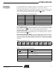
Table 1. Instruction Set for the AT25010/020/040
Instruction Name Instruction Format Operation
WREN 0000 X110 Set Write Enable Latch
WRDI 0000 X100 Reset Write Enable Latch
RDSR 0000 X101 Read Status Register
WRSR 0000 X001 Write Status Register
READ 0000 A011 Read Data from Memory Array
WRITE 0000 A010 Write Data to Memory Array
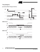
Table 2. Status Register Format
Bit 7 Bit 6 Bit 5 Bit 4 Bit 3 Bit 2 Bit 1 Bit 0
X X X X BP1 BP0 WEN RDY
Table 3. Read Status Register Bit Definition
Bit Definition
Bit 0 (RDY
)
Bit 0 = 0 (RDY
) indicates the device is READY. Bit 0 = 1 indicates the
write cycle is in progress.
Bit 1 (WEN)
Bit 1 = 0 indicates the device
is not
WRITE ENABLED. Bit 1 = 1 indicates
the device is WRITE ENABLED.
Bit 2 (BP0) See Table 4.
Bit 3 (BP1) See Table 4.
Bits 4-7 are 0s when device is not in an internal write cycle.
Bits 0-7 are 1s during an internal write cycle.