
Owner manual


5
AT25128/256
3262C–SEEPR–6/03
Serial Interface
Description
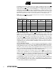
MASTER: The device that generates the serial clock.
SLAVE: Because the Serial Clock pin (SCK) is always an input, the AT25128/256
always operates as a slave.
TRANSMITTER/RECEIVER: The AT25128/256 has separate pins designated for data
transmission (SO) and reception (SI).
MSB: The Most Significant Bit (MSB) is the first bit transmitted and received.
SERIAL OP-CODE: After the device is selected with CS
going low, the first byte will
be received. This byte contains the op-code that defines the operations to be performed.
INVALID OP-CODE: If an invalid op-code is received, no data will be shifted into the
AT25128/256, and the serial output pin (SO) will remain in a high impedance state until
the falling edge of CS
is detected again. This will reinitialize the serial communication.
CHIP SELECT: The AT25128/256 is selected when the CS
pin is low. When the device
is not selected, data will not be accepted via the SI pin, and the serial output pin (SO)
will remain in a high impedance state.
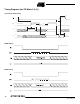
HOLD: The HOLD
pin is used in conjunction with the CS pin to select the AT25128/256.
When the device is selected and a serial sequence is underway, HOLD
can be used to
pause the serial communication with the master device without resetting the serial
sequence. To pause, the HOLD
pin must be brought low while the SCK pin is low. To
resume serial communication, the HOLD
pin is brought high while the SCK pin is low
(SCK may still toggle during HOLD
). Inputs to the SI pin will be ignored while the SO pin
is in the high impedance state.
WRITE PROTECT: The write protect pin (WP
) will allow normal read/write operations
when held high. When the WP
pin is brought low and WPEN bit is “1”, all write opera-
tions to the status register are inhibited. WP
going low while CS is still low will interrupt a
write to the status register. If the internal write cycle has already been initiated, WP
going low will have no effect on any write operation to the status register. The WP pin
function is blocked when the WPEN bit in the status register is “0”. This will allow the
user to install the AT25128/256 in a system with the WP
pin tied to ground and still be
able to write to the status register. All WP
pin functions are enabled when the WPEN bit
is set to “1”.