
Owner manual


8
AT25128/256
3262C–SEEPR–6/03
The WRSR instruction also allows the user to enable or disable the write protect (WP)
pin through the use of the Write Protect Enable (WPEN) bit. Hardware write protection is
enabled when the WP
pin is low and the WPEN bit is “1”. Hardware write protection is
disabled when
either
the WP pin is high or the WPEN bit is “0.” When the device is hard-
ware write protected, writes to the Status Register, including the Block Protect bits and
the WPEN bit, and the block-protected sections in the memory array are disabled.
Writes are only allowed to sections of the memory which are not block-protected.
NOTE: When the WPEN bit is hardware write protected, it cannot be changed back to
“0”, as long as the WP
pin is held low.
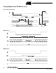
READ SEQUENCE (READ): Reading the AT25128/256 via the SO (Serial Output) pin
requires the following sequence. After the CS
line is pulled low to select a device, the
READ op-code is transmitted via the SI line followed by the byte address to be read
(Refer to Table 6). Upon completion, any data on the SI line will be ignored. The data
(D7 - D0) at the specified address is then shifted out onto the SO line. If only one byte is
to be read, the CS
line should be driven high after the data comes out. The READ
sequence can be continued since the byte address is automatically incremented and
data will continue to be shifted out. When the highest address is reached, the address
counter will roll over to the lowest address allowing the entire memory to be read in one
continuous READ cycle.
WRITE SEQUENCE (WRITE): In order to program the AT25128/256, two separate
instructions must be executed. First, the device must be write enabled via the Write
Enable (WREN) Instruction. Then a Write (WRITE) Instruction may be executed. Also,
the address of the memory location(s) to be programmed must be outside the protected
address field location selected by the Block Write Protection Level. During an internal
write cycle, all commands will be ignored except the RDSR instruction.
A Write Instruction requires the following sequence. After the CS
line is pulled low to
select the device, the WRITE op-code is transmitted via the SI line followed by the byte
address and the data (D7 - D0) to be programmed (Refer to Table 6). Programming will
start after the CS
pin is brought high. (The LOW-to-High transition of the CS pin must
occur during the SCK low time immediately after clocking in the D0 (LSB) data bit.
The READY/BUSY status of the device can be determined by initiating a READ STA-
TUS REGISTER (RDSR) Instruction. If Bit 0 = 1, the WRITE cycle is still in progress. If
Bit 0 = 0, the WRITE cycle has ended. Only the READ STATUS REGISTER instruction
is enabled during the WRITE programming cycle.
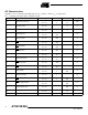
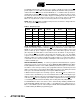
Table 5. WPEN Operation
WPEN WP WEN
Protected
Blocks
Unprotected
Blocks
Status
Register
0 X 0 Protected Protected Protected
0 X 1 Protected Writable Writable
1 Low 0 Protected Protected Protected
1 Low 1 Protected Writable Protected
X High 0 Protected Protected Protected
X High 1 Protected Writable Writable