Features • Single 1.65V - 1.
The AT25DF081 also offers a sophisticated method for protecting individual sectors against erroneous or malicious program and erase operations. By providing the ability to individually protect and unprotect sectors, a system can unprotect a specific sector to modify its contents while keeping the remaining sectors of the memory array securely protected.
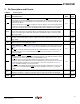
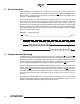
AT25DF081 2. Pin Descriptions and Pinouts Table 2-1. Symbol Pin Descriptions Name and Function Asserted State Type Low Input CS CHIP SELECT: Asserting the CS pin selects the device. When the CS pin is deasserted, the device will be deselected and normally be placed in standby mode (not Deep Power-Down mode), and the SO pin will be in a high-impedance state. When the device is deselected, data will not be accepted on the SI pin.
Figure 2-1. CS SO WP GND 8-SOIC Top View 1 2 3 4 VCC HOLD SCK SI 8 7 6 5 Figure 2-2. CS SO WP GND 8-UDFN Top View VCC HOLD 6 SCK 5 SI 1 8 2 7 3 4 Figure 2-3. 11-dBGA (Top View Through Back of Die) 1 2 3 4 A NC B VCC CS C HOLD SO D SCK WP E SI GND F NC NC 3. Block Diagram CONTROL AND PROTECTION LOGIC CS I/O BUFFERS AND LATCHES SRAM DATA BUFFER SCK INTERFACE CONTROL AND LOGIC SI Y-DECODER ADDRESS LATCH SO WP HOLD X-DECODER Y-GATING FLASH MEMORY ARRAY 4.
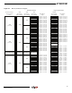
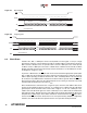
AT25DF081 Memory Architecture Diagram Block Erase Detail 64KB Block Erase (D8h Command) 32KB Block Erase (52h Command) 32KB 64KB (Sector 15) 64KB 32KB 32KB 64KB (Sector 14) 64KB ••• ••• ••• 32KB 32KB 64KB (Sector 0) 64KB 32KB 4KB Block Erase (20h Command) 4KB 4KB 4KB 4KB 4KB 4KB 4KB 4KB 4KB 4KB 4KB 4KB 4KB 4KB 4KB 4KB 4KB 4KB 4KB 4KB 4KB 4KB 4KB 4KB 4KB 4KB 4KB 4KB 4KB 4KB 4KB 4KB Block Address Range 0F F F F F h – 0F F 000h 0F E F F F h– 0F E 000h 0F DF F F h – 0F D000h 0F CF F F h – 0F C
5. Device Operation The AT25DF081 is controlled by a set of instructions that are sent from a host controller, commonly referred to as the SPI Master. The SPI Master communicates with the AT25DF081 via the SPI bus which is comprised of four signal lines: Chip Select (CS), Serial Clock (SCK), Serial Input (SI), and Serial Output (SO).
AT25DF081 Table 6-1.
7. Read Commands 7.1 Read Array The Read Array command can be used to sequentially read a continuous stream of data from the device by simply providing the SCK signal once the initial starting address has been specified. The device incorporates an internal address counter that automatically increments on every clock cycle. Two opcodes, 0Bh and 03h, can be used for the Read Array command. The use of each opcode depends on the maximum SCK frequency that will be used to read data from the device.
AT25DF081 8. Program and Erase Commands 8.1 Byte/Page Program The Byte/Page Program command allows anywhere from a single byte of data to 256 bytes of data to be programmed into previously erased memory locations. An erased memory location is one that has all eight bits set to the logical “1” state (a byte value of FFh).
Figure 8-1. Byte Program CS 0 1 2 3 4 5 6 7 8 9 10 11 12 29 30 31 32 33 34 35 36 37 38 39 SCK OPCODE SI 0 0 0 0 0 ADDRESS BITS A23-A0 0 1 0 MSB A A A A A A A A D MSB D D D D D D D MSB HIGH-IMPEDANCE SO Figure 8-2. A DATA IN Page Program CS 0 1 2 3 4 5 6 7 8 9 29 30 31 32 33 34 35 36 37 38 39 SCK OPCODE SI 0 0 0 0 0 ADDRESS BITS A23-A0 0 MSB SO 8.
AT25DF081 If the address specified by A23-A0 points to a memory location within a sector that is in the protected state, then the Block Erase command will not be executed, and the device will return to the idle state once the CS pin has been deasserted. The WEL bit in the Status Register will be reset back to the logical “0” state if the erase cycle aborts due to an incomplete address being sent or because a memory location within the region to be erased is protected.
ter be polled rather than waiting the tCHPE time to determine if the device has finished erasing. At some point before the erase cycle completes, the WEL bit in the Status Register will be reset back to the logical “0” state. The device also incorporates an intelligent erasing algorithm that can detect when a byte location fails to erase properly. If an erase error arises, it will be indicated by the EPE bit in the Status Register. Figure 8-4.
AT25DF081 9.2 Write Disable The Write Disable command is used to reset the Write Enable Latch (WEL) bit in the Status Register to the logical “0” state. With the WEL bit reset, all program, erase, Protect Sector, Unprotect Sector, and Write Status Register commands will not be executed. The Write Disable command is also used to exit the Sequential Program Mode.
A0 will be set to the logical “1” state, and the sector itself will then be protected from program and erase operations. In addition, the WEL bit in the Status Register will be reset back to the logical “0” state.
AT25DF081 As a safeguard against accidental or erroneous locking or unlocking of sectors, the Sector Protection Registers can themselves be locked from updates by using the SPRL (Sector Protection Registers Locked) bit of the Status Register (please refer to “Status Register Commands” on page 20 for more details).
Table 9-2. WP State Valid SPRL and Global Protect/Unprotect Conditions Current SPRL Value New Write Status Register Data Bit 76543210 0x0000xx 0x0001xx 0x1110xx 0x1111xx 0 New SPRL Value Protection Operation Global Unprotect – all Sector Protection Registers reset to 0 No change to current protection. No change to current protection. No change to current protection.
AT25DF081 If the desire is to only change the SPRL bit without performing a Global Protect or Global Unprotect, then the system can simply write a 0Fh to the Status Register to change the SPRL bit from a logical “1” to a logical “0” provided the WP pin is deasserted. Likewise, the system can write an F0h to change the SPRL bit from a logical “0” to a logical “1” without affecting the current sector protection status (no changes will be made to the Sector Protection Registers).
Figure 9-5. Read Sector Protection Register CS 0 1 2 3 4 5 6 7 8 9 10 11 12 29 30 31 32 33 34 35 36 37 38 39 40 SCK OPCODE SI 0 0 1 1 1 ADDRESS BITS A23-A0 1 MSB 0 0 A A A A A A A A A MSB DATA BYTE SO HIGH-IMPEDANCE D MSB 9.7 D D D D D D D D D MSB Protected States and the Write Protect (WP) Pin The WP pin is not linked to the memory array itself and has no direct effect on the protection status of the memory array.
AT25DF081 The tables below detail the various protection and locking states of the device. Table 9-4. Software Protection Register States WP Sector Protection Register n(1) Sector n(1) 0 Unprotected 1 Protected X (Don't Care) Note: 1. “n” represents a sector number Table 9-5.
10. Status Register Commands 10.1 Read Status Register The Status Register can be read to determine the device’s ready/busy status, as well as the status of many other functions such as Hardware Locking and Software Protection. The Status Register can be read at any time, including during an internally self-timed program or erase operation. To read the Status Register, the CS pin must first be asserted and the opcode of 05h must be clocked into the device.
AT25DF081 10.1.1 SPRL Bit The SPRL bit is used to control whether the Sector Protection Registers can be modified or not. When the SPRL bit is in the logical “1” state, all Sector Protection Registers are locked and cannot be modified with the Protect Sector and Unprotect Sector commands (the device will ignore these commands). In addition, the Global Protect and Global Unprotect features cannot be performed.
• Write Disable operation completes successfully • Write Status Register operation completes successfully or aborts • Protect Sector operation completes successfully or aborts • Unprotect Sector operation completes successfully or aborts • Byte/Page Program operation completes successfully or aborts • Block Erase operation completes successfully or aborts • Chip Erase operation completes successfully or aborts If the WEL bit is in the logical “1” state, it will not be reset to a logical “0” if an operation
AT25DF081 The complete one byte of data must be clocked into the device before the CS pin is deasserted, and the CS pin must be deasserted on an even byte boundary (multiples of eight bits); otherwise, the device will abort the operation, the state of the SPRL bit will not change, no potential Global Protect or Unprotect will be performed, and the WEL bit in the Status Register will be reset back to the logical “0” state. If the WP pin is asserted, then the SPRL bit can only be set to a logical “1”.
Deasserting the CS pin will terminate the Manufacturer and Device ID read operation and put the SO pin into a high-impedance state. The CS pin can be deasserted at any time and does not require that a full byte of data be read. Table 11-1. Manufacturer and Device ID Information Byte No. Data Type Value 1 Manufacturer ID 1Fh 2 Device ID (Part 1) 45h 3 Device ID (Part 2) 02h 4 Extended Device Information String Length 00h Table 11-2.
AT25DF081 11.2 Deep Power-Down During normal operation, the device will be placed in the standby mode to consume less power as long as the CS pin remains deasserted and no internal operation is in progress. The Deep Power-Down command offers the ability to place the device into an even lower power consumption state called the Deep Power-Down mode.
11.3 Resume from Deep Power-Down In order exit the Deep Power-Down mode and resume normal device operation, the Resume from Deep Power-Down command must be issued. The Resume from Deep Power-Down command is the only command that the device will recognize while in the Deep Power-Down mode. To resume from the Deep Power-Down mode, the CS pin must first be asserted and opcode of ABh must be clocked into the device. Any additional data clocked into the device after the opcode will be ignored.
AT25DF081 11.4 Hold The HOLD pin is used to pause the serial communication with the device without having to stop or reset the clock sequence. The Hold mode, however, does not have an affect on any internally self-timed operations such as a program or erase cycle. Therefore, if an erase cycle is in progress, asserting the HOLD pin will not pause the operation, and the erase cycle will continue until it is finished. The Hold mode can only be entered while the CS pin is asserted.
12. Electrical Specifications 12.1 Absolute Maximum Ratings* Temperature Under Bias ............................... -55C to +125C *NOTICE: Storage Temperature..................................... -65C to +150C All Input Voltages (including NC Pins) with Respect to Ground .....................................-0.6V to +3.8V All Output Voltages with Respect to Ground .............................-0.6V to VCC + 0.5V 12.
AT25DF081 12.4 AC Characteristics Symbol Parameter fSCK Min Max Units Serial Clock (SCK) Frequency 66 MHz fRDLF SCK Frequency for Read Array (Low Frequency – 03h opcode) 33 MHz tSCKH SCK High Time 6.8 ns SCK Low Time 6.8 ns (1) SCK Rise Time, Peak-to-Peak (Slew Rate) 0.1 V/ns tSCKF (1) SCK Fall Time, Peak-to-Peak (Slew Rate) 0.
12.5 Program and Erase Characteristics Symbol Parameter tPP tBP Typ Max Units Page Program Time (256 Bytes) 1.0 5.0 ms Byte Program Time 15 Block Erase Time tBLKE tCHPE Min (1) Chip Erase Time (1) Write Status Register Time tWRSR 4-Kbyte 50 200 32-Kbyte 350 600 64-Kbyte 600 950 8 14 sec 200 ns Max Units Notes: 1. Not 100% tested (value guaranteed by design and characterization). 12.
AT25DF081 13. AC Waveforms Figure 13-1. Serial Input Timing tCSH CS tCSLH tSCKL tCSLS tSCKH tCSHH tCSHS SCK tDS SI SO tDH MSB LSB MSB HIGH-IMPEDANCE Figure 13-2. Serial Output Timing CS tSCKH tSCKL tDIS SCK SI tOH tV tV SO Figure 13-3.
Figure 13-4. HOLD Timing – Serial Output CS SCK tHHH tHLS tHLH tHHS HOLD SI tHLQZ tHHQX SO Figure 13-5.
AT25DF081 14. Ordering Information 14.1 Ordering Code Detail – Standard Package Offerings AT 2 5 DF 0 8 1 ದ SSHN ದ B Designator Shipping Carrier Option B = Bulk (tubes) Y = Trays T = Tape and reel Product Family Operating Voltage N = 1.65V minimum (1.65V to 1.
14.3 Ordering Code Detail – Wafer Level Options A T 2 5 D F 0 8 1 ದ WB T 1 1 N Designator Operating Voltage N = 1.65V minimum (1.65V to 1.95V) Product Family Die/Wafer Backgrind Thickness 20 = 20mils 11 = 11mils Die/Wafer Carrier Option Device Density 08 = 8-megabit T = Tape and reel Interface Wafer Level Option 1 = Serial 14.
AT25DF081 15. Packaging Information 15.1 8S1 – JEDEC SOIC C 1 E E1 L N Ø TOP VIEW END VIEW e b COMMON DIMENSIONS (Unit of Measure = mm) A A1 D SIDE VIEW Notes: This drawing is for general information only. Refer to JEDEC Drawing MS-012, Variation AA for proper dimensions, tolerances, datums, etc. SYMBOL MIN A 1.35 NOM MAX – 1.75 A1 0.10 – 0.25 b 0.31 – 0.51 C 0.17 – 0.25 D 4.80 – 5.05 E1 3.81 – 3.99 E 5.79 – 6.20 e NOTE 1.27 BSC L 0.40 – 1.
15.2 8MA1 – UDFN E C Pin 1 ID SIDE VIEW D y TOP VIEW A1 A K E2 0.45 8 Option A Pin #1 Chamfer (C 0.35) 1 Pin #1 Notch (0.20 R) (Option B) 7 2 e D2 6 3 COMMON DIMENSIONS (Unit of Measure = mm) SYMBOL MIN NOM MAX A 0.45 0.55 0.60 A1 0.00 0.02 0.05 b 0.35 0.40 0.48 C 5 4 b L BOTTOM VIEW NOTE 0.152 REF D 4.90 5.00 5.10 D2 3.80 4.00 4.20 E 5.90 6.00 6.10 E2 3.20 3.40 3.60 L 0.50 0.60 0.75 y 0.00 – 0.08 K 0.20 – – e 1.
AT25DF081 16. Revision History Revision Level – Release Date History A – September 2007 Initial release B – October 2007 Changed part number ordering code to reflect NiPdAu lead finish - Changed AT25DF081-SSU-1.8 to AT25DF081-SSH-1.8 - Changed AT25DF081-MU-1.8 to AT25DF081-MH-1.8 Added lead finish details to Ordering Information table C – December 2007 Changed description from “1.8-volt Only Serial Firmware DataFlash” to “1.
Corporate Office California | USA Adesto Headquarters 1250 Borregas Avenue Sunnyvale, CA 94089 Phone: (+1) 408.400.0578 Email: contact@adestotech.com © 2012 Adesto Technologies. All rights reserved. / Rev.: 3674E–DFLASH–8/08 Adesto®, the Adesto logo, CBRAM®, and DataFlash® are registered trademarks or trademarks of Adesto Technologies. All other marks are the property of their respective owners.