
Owner's manual


11
AT25DL081 [DATASHEET]
8732D–DFLASH–12/2012
7.2 Dual-Output Read Array
The Dual-Output Read Array command is similar to the standard Read Array command and can be used to sequentially
read a continuous stream of data from the device by simply providing the clock signal once the initial starting address has
been specified. Unlike the standard Read Array command, however, the Dual-Output Read Array command allows two
bits of data to be clocked out of the device on every clock cycle, rather than just one.
The Dual-Output Read Array command can be used at any clock frequency, up to the maximum specified by f
RDDO
. To
perform the Dual-Output Read Array operation, the
CS pin must first be asserted and then the opcode 3Bh must be
clocked into the device. After the opcode has been clocked in, the three address bytes must be clocked in to specify the
location of the first byte to read within the memory array. Following the three address bytes, a single dummy byte must
also be clocked into the device.
After the three address bytes and the dummy byte have been clocked in, additional clock cycles will result in data being
output on both the SO and SIO pins. The data is always output with the MSB of a byte first and the MSB is always output
on the SO pin. During the first clock cycle, bit seven of the first data byte is output on the SO pin, while bit six of the same
data byte is output on the SIO pin. During the next clock cycle, bits five and four of the first data byte are output on the SO
and SIO pins, respectively. The sequence continues with each byte of data being output after every four clock cycles.
When the last byte (FFFFFh) of the memory array has been read, the device will continue reading from the beginning of
the array (000000h). No delays will be incurred when wrapping around from the end of the array to the beginning of the
array.
Deasserting the
CS pin will terminate the read operation and put the SO and SIO pins into a high-impedance state. The
CS pin can be deasserted at any time and does not require that a full byte of data be read.
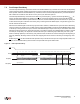
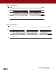
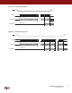
Figure 7-4. Dual-Output Read Array
SCK
CS
SI (SIO)
SO (SOI)
MSB MSB
2310
00111011
675410119812 394243414037 3833 36353431 3229 30 44 47 484645
Opcode
AAAA AAAAA
MSB
XXXXXXXX
MSB MSB MSB
D
7
D
6
D
5
D
4
D
3
D
2
D
1
D
0
D
7
D
6
D
5
D
4
D
7
D
6
D
5
D
4
D
3
D
2
D
1
D
0
Address Bits A23-A0 Don't Care
Output
Data Byte 1
Output
Data Byte 2
High-impedance