
Owner's manual


17
AT25DL081 [DATASHEET]
8732D–DFLASH–12/2012
8.4 Chip Erase
The entire memory array can be erased in a single operation by using the Chip Erase command. Before a Chip Erase
command can be started, the Write Enable command must have been previously issued to the device to set the WEL bit
of the Status Register to a Logical 1 state.
Two opcodes, 60h and C7h, can be used for the Chip Erase command. There is no difference in device functionality
when utilizing the two opcodes, so they can be used interchangeably. To perform a Chip Erase, one of the two opcodes
(60h or C7h) must be clocked into the device. Since the entire memory array is to be erased, no address bytes need to
be clocked into the device and any data clocked in after the opcode will be ignored. When the
CS pin is deasserted, the
device will erase the entire memory array. The erasing of the device is internally self-timed and should take place in a
time of t
CHPE
.
The complete opcode must be clocked into the device before the
CS pin is deasserted, and the CS pin must be
deasserted on an even byte boundary (multiples of eight bits); otherwise, no erase will be performed. In addition, if any
sector of the memory array is in the protected or locked down state, then the Chip Erase command will not be executed
and the device will return to the idle state once the
CS pin has been deasserted. The WEL bit in the Status Register will
be reset back to the Logical 0 state if the
CS pin is deasserted on uneven byte boundaries or if a sector is in the protected
or locked down state.
While the device is executing a successful erase cycle, the Status Register can be read and will indicate that the device
is busy. For faster throughput, it is recommended that the Status Register be polled rather than waiting the t
CHPE
time to
determine if the device has finished erasing. At some point before the erase cycle completes, the WEL bit in the Status
Register will be reset back to the Logical 0 state.
The device also incorporates an intelligent erase algorithm that can detect when a byte location fails to erase properly. If
an erase error occurs, it will be indicated by the EPE bit in the Status Register.
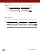
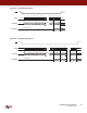
Figure 8-6. Chip Erase
SCK
CS
SI
SO
MSB
2310
CCCCCCCC
6754
Opcode
High-impedance