
Owner's manual


40
AT25DL081 [DATASHEET]
8732D–DFLASH–12/2012
11.3 Write Status Register Byte 2
The Write Status Register Byte 2 command is used to modify the RSTE and SLE bits of the Status Register. Using the
Write Status Register Byte 2 command is the only way to modify the RSTE and SLE bits in the Status Register during
normal device operation, and the SLE bit can only be modified if the sector lockdown state has not been frozen. Before
the Write Status Register Byte 2 command can be issued, the Write Enable command must have been previously issued
to set the WEL bit in the Status Register to a Logical 1.
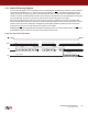
To issue the Write Status Register Byte 2 command, the CS pin must first be asserted and then the opcode 31h must be
clocked into the device followed by one byte of data. The one byte of data consists of three don’t-care bits, the RSTE bit
value, the SLE bit value, and three additional don’t-care bits (see Table 11-4). Any additional data bytes sent to the
device will be ignored. When the
CS pin is deasserted, the RSTE and SLE bits in the Status Register will be modified,
and the WEL bit in the Status Register will be reset back to a Logical 0. The SLE bit will only be modified if the Freeze
Sector Lockdown State command has not been previously issued.
The complete one byte of data must be clocked into the device before the
CS pin is deasserted, and the CS pin must be
deasserted on even byte boundaries (multiples of eight bits); otherwise, the device will abort the operation, the state of
the RSTE and SLE bits will not change, and the WEL bit in the Status Register will be reset back to the Logical 0 state.
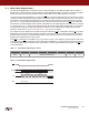
Figure 11-3. Write Status Register Byte 2
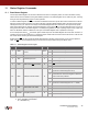
Table 11-4. Write Status Register Byte 2 Format
Bit 7 Bit 6 Bit 5 Bit 4 Bit 3 Bit 2 Bit 1 Bit 0
X X X RSTE SLE X X X
SCK
CS
SI
SO
MSB
2310
0011000
6754
Opcode
10 119814151312
1
MSB
XXXDDXXX
Status Register In
Byte 2
High-impedance