
Owner's manual


8
AT25DL081 [DATASHEET]
8732D–DFLASH–12/2012
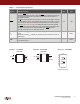
Table 6-1. Command Listing
Command Opcode
Clock
Frequency
Address
Bytes
Dummy
Bytes
Data
Bytes
Read Commands
Read Array
1Bh 0001 1011 Up to 100MHz 3 2 1+
0Bh 0000 1011 Up to 85MHz 3 1 1+
03h 0000 0011 Up to 40MHz 3 0 1+
Dual-Output Read Array 3Bh 0011 1011 Up to 85MHz 3 1 1+
Program and Erase Commands
Block Erase (4KB) 20h 0010 0000 Up to 100MHz 3 0 0
Block Erase (32KB) 52h 0101 0010 Up to 100MHz 3 0 0
Block Erase (64KB) D8h 1101 1000 Up to 100MHz 3 0 0
Chip Erase
60h 0110 0000 Up to 100MHz 0 0 0
C7h 1100 0111 Up to 100MHz 0 0 0
Byte/Page Program (1 to 256 bytes) 02h 0000 0010 Up to 100MHz 3 0 1+
Dual-Input Byte/Page Program (1 to 256 bytes) A2h 1010 0010 Up to 100MHz 3 0 1+
Program/Erase Suspend B0h 1011 0000 Up to 100MHz 0 0 0
Program/Erase Resume D0h 1101 0000 Up to 100MHz 0 0 0
Protection Commands
Write Enable 06h 0000 0110 Up to 100MHz 0 0 0
Write Disable 04h 0000 0100 Up to 100MHz 0 0 0
Protect Sector 36h 0011 0110 Up to 100MHz 3 0 0
Unprotect Sector 39h 0011 1001 Up to 100MHz 3 0 0
Global Protect/Unprotect Use Write Status Register Byte 1 Command
Read Sector Protection Registers 3Ch 0011 1100 Up to 100MHz 3 0 1+
Security Commands
Sector Lockdown 33h 0011 0011 Up to 100MHz 3 0 1
Freeze Sector Lockdown State 34h 0011 0100 Up to 100MHz 3 0 1
Read Sector Lockdown Registers 35h 0011 0101 Up to 100MHz 3 0 1+
Program OTP Security Register 9Bh 1001 1011 Up to 100MHz 3 0 1+
Read OTP Security Register 77h 0111 0111 Up to 100MHz 3 2 1+
Status Register Commands
Read Status Register 05h 0000 0101 Up to 100MHz 0 0 1+
Write Status Register Byte 1 01h 0000 0001 Up to 100MHz 0 0 1
Write Status Register Byte 2 31h 0011 0001 Up to 100MHz 0 0 1
Miscellaneous Commands
Reset F0h 1111 0000 Up to 100MHz 0 0 1
Read Manufacturer and Device ID 9Fh 1001 1111 Up to 85MHz 0 0 1 to 5
Deep Power-Down B9h 1011 1001 Up to 100MHz 0 0 0
Resume from Deep Power-Down ABh 1010 1011 Up to 100MHz 0 0 0