AT25DL161 16-Mbit, 1.65V Minimum SPI Serial Flash Memory with Dual-I/O Support DATASHEET Features Single 1.65V – 1.
1. Description The AT25DL161 is a serial interface Flash memory device designed for use in a wide variety of high-volume, consumerbased applications in which program code is shadowed from Flash memory into embedded or external RAM for execution. The flexible erase architecture of the AT25DL161, with its erase granularity as small as 4KB, makes it ideal for data storage as well, eliminating the need for additional data storage EEPROM devices.
2. Pin Descriptions and Pinouts Table 2-1. Symbol CS SCK Pin Descriptions Name and Function Chip Select: Asserting the CS pin selects the device. When the CS pin is deasserted, the device will be deselected and normally be placed in standby mode (not deep Power-Down mode) and the SO pin will be in a high-impedance state. When the device is deselected, data will not be accepted on the SI pin.
Table 2-1. Symbol Pin Descriptions (Continued) Name and Function Asserted State Type Low Input — Power — Power Hold: The HOLD pin is used to temporarily pause serial communication without deselecting or resetting the device. While the HOLD pin is asserted, transitions on the SCK pin and data on the SI pin will be ignored and the SO pin will be in a high-impedance state. HOLD The CS pin must be asserted and the SCK pin must be in the low state in order for a Hold condition to start.
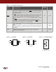
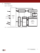
Block Diagram Figure 3-1. Block Diagram Control and Protection Logic CS SCK SI (SIO) SO (SOI) WP HOLD Note: I/O Buffers and Latches SRAM Data Buffer Interface Control and Logic Y-Decoder Address Latch 3. X-Decoder Y-Gating Flash Memory Array SIO and SOI pin naming convention is used for Dual-I/O commands.
4. Memory Array To provide the greatest flexibility, the AT25DL161 memory array can be erased in four levels of granularity, including a full Chip Erase. In addition, the array has been divided into physical sectors of uniform size, which can be individually protected from program and erase operations. The size of the physical sectors is optimized for both code and data storage applications, allowing both code and data segments to reside in their own isolated regions.
5. Device Operation The AT25DL161 is controlled by a set of instructions that are sent from a host controller, commonly referred to as the SPI master. The SPI master communicates with the AT25DL161 via the SPI bus, which is comprised of four signal lines: Chip Select (CS), Serial Clock (SCK), Serial Input (SI), and Serial Output (SO).
Table 6-1.
7. Read Commands 7.1 Read Array The Read Array command can be used to sequentially read a continuous stream of data from the device by simply providing the clock signal once the initial starting address has been specified. The device incorporates an internal address counter that automatically increments on every clock cycle. Three opcodes (1Bh, 0Bh, and 03h) can be used for the Read Array command.
Figure 7-1. Read Array – 1Bh Opcode CS 0 1 2 3 4 5 6 7 8 9 10 11 12 29 30 31 32 33 34 35 36 37 38 39 40 41 42 43 44 45 46 47 48 49 50 51 52 53 54 55 56 SCK Opcode SI 0 0 0 1 1 Address Bits A23-A0 0 1 1 A MSB A A A A A A MSB Don't Care A A X X X X X Don't Care X X X MSB X X X X X X X X MSB Data Byte 1 SO High-impedance D D D D D D D MSB D D D MSB Figure 7-2.
7.2 Dual-Output Read Array The Dual-Output Read Array command is similar to the standard Read Array command and can be used to sequentially read a continuous stream of data from the device by simply providing the clock signal once the initial starting address has been specified. Unlike the standard Read Array command, however, the Dual-Output Read Array command allows two bits of data to be clocked out of the device on every clock cycle, rather than just one.
8. Program and Erase Commands 8.1 Byte/Page Program The Byte/Page program command allows anywhere from a single byte of data to 256 bytes of data to be programmed into previously erased memory locations. An erased memory location is one that has all eight bits set to the Logical 1 state (a byte value of FFh).
Figure 8-1. Byte Program CS 0 1 2 3 4 5 6 7 8 9 10 11 12 29 30 31 32 33 34 35 36 37 38 39 SCK Opcode SI 0 0 0 0 0 Address Bits A23-A0 0 1 0 MSB SO A A A A A A A Data In A A MSB D D D D D D D D MSB High-impedance Figure 8-2.
8.2 Dual-Input Byte/Page Program The Dual-Input Byte/Page Program command is similar to the standard Byte/Page Program command and can be used to program anywhere from a single byte of data up to 256 bytes of data into previously erased memory locations. Unlike the standard byte/page program command, however, the Dual-Input Byte/Page Program command allows two bits of data to be clocked into the device on every clock cycle rather than just one.
Figure 8-3. Dual-Input Byte Program CS 0 1 2 3 4 5 6 7 8 9 10 11 12 29 30 31 32 33 34 35 SCK Opcode SI (SIO) 1 0 1 0 0 0 1 0 A MSB SO (SOI) Input Data Byte Address Bits A23-A0 A A A A A A A A D6 D4 D2 D0 MSB High-impedance D7 D5 D3 D1 MSB Figure 8-4.
8.3 Block Erase A block of 4, 32, or 64KB can be erased (all bits set to the Logical 1 state) in a single operation by using one of three different opcodes for the Block Erase command. An opcode of 20h is used for a 4KB erase, an opcode of 52h is used for a 32KB erase, and an opcode of D8h is used for a 64KB erase. Before a Block Erase command can be started, the Write Enable command must have been previously issued to the device to set the WEL bit of the Status Register to a Logical 1 state.
8.4 Chip Erase The entire memory array can be erased in a single operation by using the Chip Erase command. Before a Chip Erase command can be started, the Write Enable command must have been previously issued to the device to set the WEL bit of the Status Register to a Logical 1 state. Two opcodes, 60h and C7h, can be used for the Chip Erase command. There is no difference in device functionality when utilizing the two opcodes, so they can be used interchangeably.
8.5 Program/Erase Suspend In some code-plus-data storage applications, it is often necessary to process certain high-level system interrupts that require relatively immediate reading of code or data from the Flash memory. In such an instance, it may not be possible for the system to wait the microseconds or milliseconds required for the Flash memory to complete a program or erase cycle.
. Table 8-1.
8.6 Program/Erase Resume The Program/Erase Resume command allows a suspended program or erase operation to be resumed and continue programming a Flash page or erasing a Flash memory block from where it left off. As with the Program/Erase Suspend command, the Write Enable command does not need to be issued prior to the Program/Erase Resume command being issued. Therefore, the Program/Erase Resume command operates independently of the state of the WEL bit in the Status Register.
9. Protection Commands and Features 9.1 Write Enable The Write Enable command is used to set the Write Enable Latch (WEL) bit in the Status Register to a Logical 1 state. The WEL bit must be set before a Byte/Page Program, Erase, Protect Sector, Unprotect Sector, Sector Lockdown, Freeze Sector Lockdown State, Program OTP Security Register, Write Status Register, or Write Configuration Register command can be executed.
9.2 Write Disable The Write Disable command is used to reset the Write Enable Latch (WEL) bit in the Status Register to the Logical 0 state. With the WEL bit reset, all Byte/Page Program, Erase, Protect Sector, Unprotect Sector, Sector Lockdown, Freeze Sector Lockdown State, Program OTP Security Register, Write Status Register, and Write Configuration Register commands will not be executed. Other conditions can also cause the WEL bit to be reset.
9.3 Protect Sector Every physical 64KB sector of the device has a corresponding single-bit Sector Protection Register that is used to control the software protection of a sector. Upon device power-up, each Sector Protection Register will default to the Logical 1 state indicating that all sectors are protected and cannot be programmed or erased. Issuing the Protect Sector command to a particular sector address will set the corresponding Sector Protection Register to the Logical 1 state.
9.4 Unprotect Sector Issuing the Unprotect Sector command to a particular sector address will reset the corresponding Sector Protection Register to the Logical 0 state (see Table 9-1 for Sector Protection Register values). Every physical sector of the device has a corresponding single-bit Sector Protection Register that is used to control the software protection of a sector.
9.5 Global Protect/Unprotect The Global Protect and Global Unprotect features can work in conjunction with the Protect Sector and Unprotect Sector functions. Example: A system can globally protect the entire memory array and then use the Unprotect Sector command to individually unprotect certain sectors and individually reprotect them later by using the Protect Sector command. Likewise, a system can globally unprotect the entire memory array and then individually protect certain sectors as needed.
Table 9-2.
9.6 Read Sector Protection Registers The Sector Protection Registers can be read to determine the current software protection status of each sector. Reading the Sector Protection Registers, however, will not determine the status of the WP pin. To read the Sector Protection Register for a particular sector, the CS pin must first be asserted and then the opcode 3Ch must be clocked in. Once the opcode has been clocked in, three address bytes designating any address within the sector must be clocked in.
9.7 Protected States and the Write Protect (WP) Pin The WP pin is not linked to the memory array itself and has no direct effect on the protection status or lockdown status of the memory array. Instead, the WP pin, in conjunction with the SPRL (Sector Protection Registers Locked) bit in the Status Register, is used to control the hardware locking mechanism of the device.
10. Security Commands 10.1 Sector Lockdown Certain applications require that portions of the Flash memory array be permanently protected against malicious attempts at altering program code, data modules, security information or encryption/decryption algorithms, keys, and routines. To address these applications, the device incorporates a sector lockdown mechanism that allows any combination of individual 64KB sectors to be permanently locked so that they become read-only.
Figure 10-1. Sector Lockdown CS 0 1 2 3 4 5 6 7 8 9 29 30 31 32 33 34 35 36 37 38 39 SCK Opcode SI 0 0 1 1 0 Address Bits A23-A0 0 1 1 A MSB SO 10.
10.3 Read Sector Lockdown Registers The Sector Lockdown Registers can be read to determine the current lockdown status of each physical 64KB sector. To read the Sector Lockdown Register for a particular 64KB sector, the CS pin must first be asserted and then the opcode 35h must be clocked in. Once the opcode has been clocked in, three address bytes designating any address within the 64KB sector must be clocked in.
10.4 Program OTP Security Register The device contains a specialized OTP (One-Time Programmable) Security Register that can be used for purposes such as unique device serialization, system-level Electronic Serial Number (ESN) storage, locked key storage, etc. The OTP Security Register is independent of the main Flash memory array and is comprised of a total of 128 bytes of memory divided into two portions.
The three address bytes and at least one complete byte of data must be clocked into the device before the CS pin is deasserted, and the CS pin must be deasserted on even byte boundaries (multiples of eight bits); otherwise, the device will abort the operation and the user-programmable portion of the OTP Security Register will not be programmed.
10.5 Read OTP Security Register The OTP Security Register can be sequentially read in a similar fashion to the Read Array operation up to the maximum clock frequency specified by fMAX. To read the OTP Security Register, the CS pin must first be asserted and then the opcode 77h must be clocked into the device. After the opcode has been clocked in, the three address bytes must be clocked in to specify the starting address location of the first byte to read within the OTP Security Register.
11. Status Register Commands 11.1 Read Status Register The two-byte Status Register can be read to determine the device’s ready/busy status, as well as the status of many other functions such as hardware locking and software protection. The Status Register can be read at any time, including during an internally self-timed program or erase operation. To read the Status Register, the CS pin must first be asserted and then the opcode 05h must be clocked into the device.
Table 11-2.
11.1.2 EPE Bit The EPE bit indicates whether the last erase or program operation completed successfully or not. If at least one byte during the erase or program operation did not erase or program properly, then the EPE bit will be set to the Logical 1 state.
11.1.6 RSTE Bit The RSTE bit is used to enable or disable the Reset command. When the RSTE bit is in the Logical 0 state (the default state after power-up), the Reset command is disabled and any attempts to reset the device using the Reset command will be ignored. When the RSTE bit is in the Logical 1 state, the Reset command is enabled. The RSTE bit will retain its state as long as power is applied to the device.
11.2 Write Status Register Byte 1 The Write Status Register Byte 1 command is used to modify the SPRL bit of the Status Register and/or to perform a Global Protect or Global Unprotect operation. Before the Write Status Register Byte 1 command can be issued, the Write Enable command must have been previously issued to set the WEL bit in the Status Register to a Logical 1.
11.3 Write Status Register Byte 2 The Write Status Register Byte 2 command is used to modify the RSTE and SLE bits of the Status Register. Using the Write Status Register Byte 2 command is the only way to modify the RSTE and SLE bits in the Status Register during normal device operation, and the SLE bit can only be modified if the sector lockdown state has not been frozen.
12. Other Commands and Functions 12.1 Reset In some applications, it may be necessary to prematurely terminate a program or erase cycle rather than wait the hundreds of microseconds or milliseconds necessary for the program or erase operation to complete normally. The Reset command allows a program or erase operation in progress to be ended abruptly and returns the device to an idle state.
12.2 Read Manufacturer and Device ID Identification information can be read from the device to enable systems to electronically query and identify the device while it is in the system. The identification method and the command opcode comply with the JEDEC standard for “Manufacturer and Device ID Read Methodology for SPI Compatible Serial Interface Memory Devices”.
Figure 12-2. Read Manufacturer and Device ID CS 0 6 7 8 14 15 16 22 23 24 30 31 32 38 39 40 46 SCK Opcode SI SO 9Fh High-impedance Note: Each transition 1Fh 46h 03h 01h 00h Manufacturer ID Device ID Byte 1 Device ID Byte 2 EDI String Length EDI Data Byte 1 shown for SI and SO represents one byte (8 bits).
12.3 Deep Power-Down During normal operation, the device will be placed in the standby mode to consume less power as long as the CS pin remains deasserted and no internal operation is in progress. The Deep Power-Down command offers the ability to place the device into an even lower power consumption state called the Deep Power-Down mode.
12.4 Resume from Deep Power-Down In order to exit the Deep Power-Down mode and resume normal device operation, the Resume from Deep Power-Down command must be issued. The Resume from Deep Power-Down command is the only command that the device will recognize while in the Deep Power-Down mode. To resume from the Deep Power-Down mode, the CS pin must first be asserted and then the opcode ABh must be clocked into the device. Any additional data clocked into the device after the opcode will be ignored.
12.5 Hold The HOLD pin is used to pause the serial communication with the device without having to stop or reset the clock sequence. The Hold mode, however, does not have an affect on any internally self-timed operations such as a program or erase cycle. Therefore, if an erase cycle is in progress, asserting the HOLD pin will not pause the operation and the erase cycle will continue until it is finished. The Hold mode can only be entered while the CS pin is asserted.
13. RapidS Implementation To implement RapidS and operate at clock frequencies higher than what can be achieved in a viable SPI implementation, a full clock cycle can be used to transmit data back and forth across the serial bus. The AT25DL161 is designed to always clock its data out on the falling edge of the SCK signal and clock data in on the rising edge of SCK.
14. Electrical Specifications 14.1 Absolute Maximum Ratings* Temperature under Bias . . . . . . . . . . -55C to +125C Storage Temperature. . . . . . . . . . . . . -65C to +150C All input voltages (including NC pins) with respect to ground . . . . . . . . . . . . . .-0.6V to +4.1V All output voltages with respect to ground . . . . . . . . . .-0.6V to VCC + 0.5V 14.2 *Notice: Stresses beyond those listed under “Absolute Maximum Ratings” may cause permanent damage to the device.
14.4 AC Characteristics – Maximum Clock Frequencies Symbol Parameter Min Max Units RapidS and SPI Operation 14.
14.6 Program and Erase Characteristics Symbol Parameter tPP(1) Page Program Time (256 bytes) tBP Byte Program Time tBLKE(1) tCHPE(1)(2) Chip Erase Time tSUSP Suspend Time tRES Resume Time tOTPP(1) OTP Security Register Program Time tWRSR(2) Write Status Register Time 2. 14.8 Typ Max Units 1.0 3.0 ms 8 Block Erase Time Notes: 1. 14.
15. AC Waveforms Figure 15-1. Serial Input Timing tCSH CS tCSLH tCLKL tCSLS tCLKH tCSHH tCSHS SCK tDS tDH SI SO MSB LSB MSB High-impedance Figure 15-2. Serial Output Timing CS tCLKH tCLKL tDIS SCK SI tOH tV tV SO Figure 15-3.
Figure 15-4. HOLD Timing – Serial Input CS SCK tHHH tHLS tHLH tHHS tHLH tHHS HOLD SI SO High-impedance Figure 15-5.
16. Ordering Information 16.1 Ordering Code Detail AT 2 5DL 1 6 1 – SSH N –B Designator Shipping Carrier Option B = Bulk (tubes) Y = Bulk (trays) T = Tape and reel Product Family Operating Voltage N = 1.65V minimum (1.65V to 1.95V) Device Density Device Grade 16 = 16-megabit H = Green, NiPdAu lead finish, Industrial temperature range (–40°C to +85°C) U = Green, Matte Sn or Sn alloy, Industrial temperature range (–40°C to +85°C) Interface 1 = Serial Package Option SS = 8-lead, 0.
17. Packaging Information 17.1 8S1 — 8-lead JEDEC SOIC C 1 E E1 L N Ø TOP VIEW END VIEW e b COMMON DIMENSIONS (Unit of Measure = mm) A A1 D SIDE VIEW Notes: This drawing is for general information only. Refer to JEDEC Drawing MS-012, Variation AA for proper dimensions, tolerances, datums, etc. SYMBOL MIN A 1.35 NOM MAX – 1.75 A1 0.10 – 0.25 b 0.31 – 0.51 C 0.17 – 0.25 D 4.80 – 5.05 E1 3.81 – 3.99 E 5.79 – 6.20 e NOTE 1.27 BSC L 0.40 – 1.
17.2 8MA1 — 8-pad UDFN E C Pin 1 ID SIDE VIEW D y TOP VIEW A1 A K E2 0.45 8 Option A Pin #1 Chamfer (C 0.35) 1 Pin #1 Notch (0.20 R) (Option B) 7 2 e D2 6 3 5 4 COMMON DIMENSIONS (Unit of Measure = mm) SYMBOL MIN NOM MAX A 0.45 0.55 0.60 A1 0.00 0.02 0.05 b 0.35 0.40 0.48 C b L BOTTOM VIEW NOTE 0.152 REF D 4.90 5.00 5.10 D2 3.80 4.00 4.20 E 5.90 6.00 6.10 E2 3.20 3.40 3.60 e 1.27 L 0.50 0.60 0.75 y 0.00 – 0.08 K 0.
17.3 8U-4 — 8-ball WLCSP Bottom View Top View d 0.015 4X -A- j j 1.887 MAX PIN A1 CORNER n n 0.015 m C 0.050 m C A B PIN A1 2 Ø0.290±0.0300 1 -B- A B 3.038 MAX 0.500 C D 1.500 0.500 0.200±0.025 0.409 MAX 2 0.140 MIN Side View 1. Dimension of ball is measured at the maximum ball diameter in a plane parallet to the seating plane. 2. Planarity applied to whole wafer. d 0.075 -C- BALL COORDINANCE TABULATION Ball Signal x-coord y-coord A2 CSBPAD -0.250 0.750 0.750 A1 vdd! 0.
18. Revision History Doc. Rev. Date Comments 8795E 12/2012 Add labels to pins in dBGA package 8795D 12/2012 Update to Adesto. 8795C 09/2012 Add WLCSP package drawing. Removed preliminary status. Updated template and Adesto logo. Decreased IDPD maximum from 14μA to 10μA. 8795B 05/2012 Decreased FRDDO maximum from 85μA to 66μA. Various typopgraphical edits throughout document. 8795A 03/2012 Initial document release.
Corporate Office California | USA Adesto Headquarters 1250 Borregas Avenue Sunnyvale, CA 94089 Phone: (+1) 408.400.0578 Email: contact@adestotech.com © 2012 Adesto Technologies. All rights reserved. / Rev.: 8795E–DFLASH–12/2012 Adesto®, the Adesto logo, CBRAM®, and DataFlash® are registered trademarks or trademarks of Adesto Technologies. All other marks are the property of their respective owners.