
User guide


14
AT25DL161 [DATASHEET]
8795E–DFLASH–12/2012
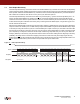
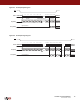
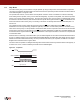
8.2 Dual-Input Byte/Page Program
The Dual-Input Byte/Page Program command is similar to the standard Byte/Page Program command and can be used
to program anywhere from a single byte of data up to 256 bytes of data into previously erased memory locations. Unlike
the standard byte/page program command, however, the Dual-Input Byte/Page Program command allows two bits of
data to be clocked into the device on every clock cycle rather than just one.
Before the Dual-Input Byte/Page Program command can be started, the Write Enable command must have been
previously issued to the device (see “Write Enable” on page 21) to set the Write Enable Latch (WEL) bit of the Status
Register to a Logical 1 state. To perform a Dual-Input Byte/Page Program command, an A2h opcode must be clocked
into the device followed by the three address bytes denoting the first location of the memory array to begin programming
at. After the address bytes have been clocked in, data can then be clocked into the device two bits at a time on both the
SOI and SI pins.
The data is always input with the MSB of a byte first, and the MSB is always input on the SOI pin. During the first clock
cycle, bit 7 of the first data byte is input on the SOI pin while bit 6 of the same data byte is input on the SI pin. During the
next clock cycle, bits 5 and 4 of the first data byte are input on the SOI and SI pins, respectively. The sequence continues
with each byte of data being input after every four clock cycles. Like the standard Byte/Page Program command, all data
clocked into the device are stored in an internal buffer.
If the starting memory address denoted by A23-A0 does not fall on an even 256-byte page boundary (A7-A0 are
not all 0), then special circumstances regarding which memory locations are to be programmed will apply. In this
situation, any data that are sent to the device that go beyond the end of the page will wrap around to the beginning of the
same page. In addition, if more than 256 bytes of data are sent to the device, then only the last 256 bytes sent will be
latched into the internal buffer.
Example: If the starting address denoted by A23-A0 is 0000FEh and three bytes of data are sent to the device, then
the first two bytes of data will be programmed at addresses 0000FEh and 0000FFh, while the last byte of
data will be programmed at address 000000h. The remaining bytes in the page (addresses 000001h
through 0000FDh) will not be programmed and will remain in the erased state (FFh).
When the
CS pin is deasserted, the device will program the data stored in the internal buffer into the appropriate memory
array locations based on the starting address specified by A23-A0 and the number of data bytes sent to the device. If
fewer than 256 bytes of data are sent to the device, then the remaining bytes within the page will not be programmed and
will remain in the erased state (FFh). The programming of the data bytes is internally self-timed and should take place in
a time of t
PP
or t
BP
if only programming a single byte.
The three address bytes and at least one complete byte of data must be clocked into the device before the
CS pin is
deasserted, and the
CS pin must be deasserted on even byte boundaries (multiples of eight bits); otherwise, the device
will abort the operation and no data will be programmed into the memory array. In addition, if the address specified by
A23-A0 points to a memory location within a sector that is in the protected state (see “Protect Sector” on page 23) or
locked down (see “Sector Lockdown” on page 29), then the Byte/Page Program command will not be executed, and the
device will return to the idle state once the
CS pin has been deasserted. The WEL bit in the Status Register will be reset
back to the Logical 0 state if the program cycle aborts due to an incomplete address being sent, an incomplete byte of
data being sent, the
CS pin being deasserted on uneven byte boundaries, or because the memory location to be
programmed is protected or locked down.
While the device is programming, the Status Register can be read and will indicate that the device is busy. For faster
throughput, it is recommended that the Status Register be polled rather than waiting the t
BP
or t
PP
time to determine if the
data bytes have finished programming. At some point before the program cycle completes, the WEL bit in the Status
Register will be reset back to the Logical 0 state.
The device also incorporates an intelligent programming algorithm that can detect when a byte location fails to program
properly. If a programming error arises, it will be indicated by the EPE bit in the Status Register.