
User guide


42
AT25DL161 [DATASHEET]
8795E–DFLASH–12/2012
12.2 Read Manufacturer and Device ID
Identification information can be read from the device to enable systems to electronically query and identify the device
while it is in the system. The identification method and the command opcode comply with the JEDEC standard for
“Manufacturer and Device ID Read Methodology for SPI Compatible Serial Interface Memory Devices”. The type of
information that can be read from the device includes the JEDEC-defined Manufacturer ID, the vendor-specific
Device ID, and the vendor-specific Extended Device Information.
The Read Manufacturer and Device ID command is limited to a maximum clock frequency of f
CLK
. Since not all Flash
devices are capable of operating at very high clock frequencies, applications should be designed to read the
identification information from the devices at a reasonably low clock frequency to ensure that all devices to be used in the
application can be identified properly. Once the identification process is complete, the application can then increase the
clock frequency to accommodate specific Flash devices that are capable of operating at the higher clock frequencies.
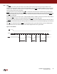
To read the identification information, the CS pin must first be asserted and then the opcode 9Fh must be clocked into
the device. After the opcode has been clocked in, the device will begin outputting the identification data on the SO pin
during the subsequent clock cycles. The first byte to be output will be the Manufacturer ID, followed by two bytes of
Device ID information. The fourth byte output will be the Extended Device Information (EDI) String Length, which will be
01h indicating that one byte of EDI data follows. After the one byte of EDI data is output, the SO pin will go into a
high-impedance state; therefore, additional clock cycles will have no affect on the SO pin and no data will be output. As
indicated in the JEDEC standard, reading the EDI String Length and any subsequent data is optional.
Deasserting the
CS pin will terminate the Manufacturer and Device ID Read operation and put the SO pin into a
high-impedance state. The
CS pin can be deasserted at any time and does not require that a full byte of data be read.
Table 12-1. Manufacturer and Device ID Information
Byte No. Data Type Value
1 Manufacturer ID 1Fh
2 Device ID (Byte 1) 46h
3 Device ID (Byte 2) 03h
4 [Optional to Read] Extended Device Information (EDI) String Length 01h
5 [Optional to Read] EDI Byte 1 00h
Table 12-2. Manufacturer and Device ID Details
Data Type Bit 7 Bit 6 Bit 5 Bit 4 Bit 3 Bit 2 Bit 1 Bit 0
Hex
Value Details
Manufacturer ID
JEDEC Assigned Code
1Fh JEDEC code: 0001 1111 (1Fh for Adesto)
0 0 0 1 1 1 1 1
Device ID (Byte 1)
Family Code Density Code
46h
Family code: 010 (SPI or Dual-I/O)
Density code: 00110 (16-Mbit)
0 1 0 0 0 1 1 0
Device ID (Byte 2)
Sub Code Product Variant
03h
Sub code: 000 (Standard Series)
Product variant: 00011
0 0 0 0 0 0 1 1
Table 12-3. EDI Data
Byte Number Bit 7 Bit 6 Bit 5 Bit 4 Bit 3 Bit 2 Bit 1 Bit 0
Hex
Value Details
1
RFU Device Revision
00h
RFU: Reserved for future use
Device revision: 00000 (Initial version)
0 0 0 0 0 0 0 0