
Owner manual

54
AT25DQ321 [DATASHEET]
8718D–DFLASH–12/2012
13. Electrical Specifications
13.1 Absolute Maximum Ratings*
13.2 DC and AC Operating Range
13.3 DC Characteristics
Temperature under Bias . . . . . . . . . . -55C to +125C
Storage Temperature . . . . . . . . . . . . -65C to +150C
All Input Voltages (including NC Pins)
with Respect to Ground . . . . . . . . . . . . .-0.6V to +4.1V
All Output Voltages
with Respect to Ground . . . . . . . . .-0.6V to V
CC
+ 0.5V
*Notice: Stresses beyond those listed under “Absolute Maximum
Ratings” may cause permanent damage to the device.
Functional operation of the device at these ratings or any
other conditions beyond those indicated in the operational
sections of this specification is not implied. Exposure to
absolute maximum rating conditions for extended periods
may affect device reliability. Voltage extremes referenced in
the "Absolute Maximum Ratings" are intended to
accommodate short duration undershoot/overshoot
conditions and does not imply or guarantee functional device
operation at these levels for any extended period of time.
AT25DQ321
Operating Temperature (Case) Industrial -40C to 85C
V
CC
Power Supply 2.7V to 3.6V
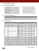
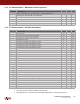
Symbol Parameter Condition Min Typ Max Units
I
SB
Standby Current
CS, WP, HOLD = V
CC
,
All inputs at CMOS levels
25 50 μA
I
DPD
Deep Power-Down Current
CS, WP, HOLD = V
CC
,
All inputs at CMOS levels
5 10 μA
I
CC1
Active Current, Read Operation
f = 100 MHz; I
OUT
= 0mA;
CS = V
IL
, V
CC
= Max
12 19
mA
f = 85 MHz; I
OUT
= 0mA;
CS = V
IL
, V
CC
= Max
10 17
f = 66 MHz; I
OUT
= 0mA;
CS = V
IL
, V
CC
= Max
8 14
f = 50 MHz; I
OUT
= 0mA;
CS = V
IL
, V
CC
= Max
7 12
f = 33 MHz; I
OUT
= 0mA;
CS = V
IL
, V
CC
= Max
6 10
f = 20 MHz; I
OUT
= 0mA;
CS = V
IL
, V
CC
= Max
5 8
I
CC2
Active Current, Program Operation CS = V
CC
, V
CC
= Max 10 20 mA
I
CC3
Active Current, Erase Operation CS = V
CC
, V
CC
= Max 12 20 mA
I
LI
Input Leakage Current V
IN
= CMOS levels 1 μA
I
LO
Output Leakage Current V
OUT
= CMOS levels 1 μA
V
IL
Input Low Voltage 0.3 x V
CC
V
V
IH
Input High Voltage 0.7 x V
CC
V
V
OL
Output Low Voltage I
OL
= 1.6mA; V
CC
= Min 0.4 V
V
OH
Output High Voltage I
OH
= -100μA; V
CC
= Min V
CC
- 0.2V V