
User guide


7
AT25F512/1024
1440P–SEEPR–6/04
Functional
Description
The AT25F512/1024 is designed to interface directly with the synchronous serial periph-
eral interface (SPI) of the 6800 type series of microcontrollers.
The AT25F512/1024 utilizes an 8-bit instruction register. The list of instructions and their
operation codes are contained in Table 1. All instructions, addresses, and data are
transferred with the MSB first and start with a high-to-low transition.
Write is defined as program and/or erase in this specification. The following commands,
PROGRAM, SECTOR ERASE, CHIP ERASE, and WRSR are write instructions for
AT25F512/1024.
WRITE ENABLE (WREN): The device will power up in the write disable state when V
CC
is applied. All write instructions must therefore be preceded by the WREN instruction.
WRITE DISABLE (WRDI): To protect the device against inadvertent writes, the WRDI
instruction disables all write commands. The WRDI instruction is independent of the sta-
tus of the WP
pin.
READ STATUS REGISTER (RDSR): The RDSR instruction provides access to the sta-
tus register. The READY/BUSY and write enable status of the device can be determined
by the RDSR instruction. Similarly, the Block Write Protection bits indicate the extent of
protection employed. These bits are set by using the WRSR instruction. During internal
write cycles, all other commands will be ignored except the RDSR instruction.
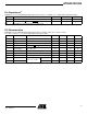
Table 1. Instruction Set for the AT25F512/1024
Instruction Name
Instruction
Format Operation
WREN 0000 X110 Set Write Enable Latch
WRDI 0000 X100 Reset Write Enable Latch
RDSR 0000 X101 Read Status Register
WRSR 0000 X001 Write Status Register
READ 0000 X011 Read Data from Memory Array
PROGRAM 0000 X010 Program Data Into Memory Array
SECTOR ERASE 0101 X010 Erase One Sector in Memory Array
CHIP ERASE 0110 X010 Erase All Sectors in Memory Array
RDID 0001 X101 Read Manufacturer and Product ID
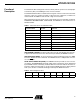
Table 2. Status Register Format
Bit 7 Bit 6 Bit 5 Bit 4 Bit 3 Bit 2 Bit 1 Bit 0
WPEN X X X BP1 BP0 WEN RDY