
User guide


8
AT25F512/1024
1440P–SEEPR–6/04
READ PRODUCT ID (RDID): The RDID instruction allows the user to read the manufac-
turer and product ID of the device. The first byte after the instruction will be the
manufacturer code (1FH = ATMEL), followed by the device code.
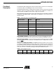
WRITE STATUS REGISTER (WRSR): The WRSR instruction allows the user to select
one of four levels of protection for the AT25F1024. The AT25F1024 is divided into four
sectors where the top quarter (1/4), top half (1/2), or all of the memory sectors can be
protected (locked out) from write. The AT25F512 is divided into 2 sectors where all of
the memory sectors can be protected (locked out) from write. Any of the locked-out sec-
tors will therefore be READ only. The locked-out sector and the corresponding status
register control bits are shown in Table 4.
The three bits, BP0, BP1, and WPEN, are nonvolatile cells that have the same proper-
ties and functions as the regular memory cells (e.g., WREN, t
WC
, RDSR).
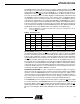
Table 3. Read Status Register Bit Definition
Bit Definition
Bit 0 (RDY)
Bit 0 = 0 (RDY
) indicates the device is READY. Bit 0 = 1 indicates the
write cycle is in progress.
Bit 1 (WEN)
Bit 1 = 0 indicates the device is not WRITE ENABLED. Bit 1 = 1 indicates
the device is WRITE ENABLED.
Bit 2 (BP0) See Table 4.
Bit 3 (BP1) See Table 4.
Bits 4-6 are 0s when device is not in an internal write cycle.
Bit 7 (WPEN) See Table 5.
Bits 0-7 are 1s during an internal write cycle.
Table 4. Block Write Protect Bits
Level
Status Register Bits AT25F512 AT25F1024
BP1 BP0
Array Addresses
Locked Out
Locked-out
Sector(s)
Array Addresses
Locked Out
Locked-out
Sector(s)
000
None None
None None
1(1/4) 0 1 018000 - 01FFFF Sector 4
2(1/2) 1 0 010000 - 01FFFF Sector 3, 4
3(All) 1 1 000000 - 00FFFF
All sectors
(1 - 2)
000000 - 01FFFF
All sectors
(1 - 4)