
Instruction Manual


10
3600H–DFLASH–11/2012
AT26DF081A
reset back to the logical “0” state if the program cycle aborts due to an incomplete address being
sent, an incomplete byte of data being sent, or because the memory location to be programmed
is protected.
While the device is programming, the Status Register can be read and will indicate that the
device is busy. For faster throughput, it is recommended that the Status Register be polled
rather than waiting the t
PP
time to determine if the data bytes have finished programming. At
some point before the program cycle completes, the WEL bit in the Status Register will be reset
back to the logical “0” state.
The device also incorporates an intelligent programming algorithm that can detect when a byte
location fails to program properly. If a programming error arises, it will be indicated by the EPE
bit in the Status Register.
The Byte/Page Program mode is the default programming mode after the device powers-up or
resumes from a device reset.
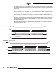
Figure 8-1. Byte Program
Figure 8-2. Page Program
SCK
CS
SI
SO
MSB MSB
2 310
00000010
6754101198 12 3937 3833 36353431 322930
OPCODE
HIGH-IMPEDANCE
AAAA AAAA A
MSB
DDDDDDDD
ADDRESS BITS A23-A0 DATA IN
SCK
CS
SI
SO
MSB MSB
2 310
00000010
6754 983937 3833 36353431 322930
OPCODE
HIGH-IMPEDANCE
AA AAAA
MSB
DDDDDDDD
ADDRESS BITS A23-A0 DATA IN BYTE 1
MSB
DDDDDDDD
DATA IN BYTE n